Introduction to Printed Circuit Boards
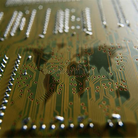
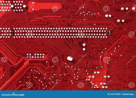
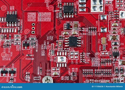
In the world of electronics and engineering, Printed Circuit Boards (PCBs) play a crucial role in the functionality and performance of various devices. A PCB is a flat board made of insulating material, such as fiberglass or plastic, with conductive pathways etched or printed onto its surface. These pathways, known as traces, connect electronic components like resistors, capacitors, and integrated circuits, allowing them to communicate and function together as a complete electronic system.
History of PCBs
The concept of PCBs dates back to the early 20th century when inventors began exploring ways to simplify the wiring of electronic devices. In 1936, Austrian engineer Paul Eisler invented the first printed circuit as part of a radio set. However, it wasn’t until the 1950s that PCBs gained widespread adoption in the electronics industry, particularly in military and aerospace applications.
Advantages of PCBs
PCBs offer numerous advantages over traditional point-to-point wiring:
- Compact size: PCBs allow for the miniaturization of electronic devices by efficiently organizing components and reducing the space required for wiring.
- Reliability: The use of PCBs minimizes the risk of loose connections and short circuits, leading to more reliable and stable electronic systems.
- Mass production: PCBs can be easily replicated and mass-produced, reducing manufacturing costs and time.
- Improved signal integrity: The precise layout and controlled impedance of PCB traces ensure better signal integrity and reduced electromagnetic interference (EMI).
PCB Manufacturing Process
The manufacturing process of PCBs involves several key steps:
PCB Design
The first step in creating a PCB is designing the circuit schematic and layout using specialized software like Altium Designer, Eagle, or KiCad. The design process involves:
- Schematic capture: Creating a graphical representation of the electronic circuit, specifying components and their interconnections.
- Component placement: Arranging the components on the board layout in a way that optimizes space, signal integrity, and manufacturability.
- Routing: Defining the conductive paths (traces) that connect the components, considering factors such as trace width, spacing, and impedance.
PCB Fabrication
Once the design is finalized, the PCB is ready for fabrication. The fabrication process typically includes the following steps:
- Substrate preparation: Cutting the insulating substrate material (e.g., fiberglass) to the desired size and shape.
- Copper cladding: Laminating a thin layer of copper foil onto the substrate.
- Photoresist application: Coating the copper layer with a light-sensitive photoresist material.
- Exposure and development: Exposing the photoresist to UV light through a photomask, which contains the PCB layout pattern. The exposed areas of the photoresist are then removed using a developer solution.
- Etching: Removing the unwanted copper areas using an etchant solution, leaving only the desired conductive traces.
- Drilling: Creating holes for through-hole components and vias (vertical interconnect access) using a drill or laser.
- Soldermask and silkscreen: Applying a protective soldermask layer and printing component labels and markings using silkscreen.
- Surface finish: Adding a surface finish, such as HASL (Hot Air Solder Leveling) or ENIG (Electroless Nickel Immersion Gold), to protect the exposed copper and improve solderability.
PCB Assembly
After the PCB is fabricated, the electronic components are attached to the board through a process called PCB assembly. There are two primary methods for PCB assembly:
- Through-hole assembly: Components with long leads are inserted into holes drilled in the PCB and soldered onto the opposite side.
- Surface-mount assembly: Components with small metal pads or leads are placed directly onto the surface of the PCB and soldered using a reflow oven or wave soldering machine.
PCB Types and Applications
PCBs come in various types and are used in a wide range of applications. Some common types of PCBs include:
Single-layer PCBs
Single-layer PCBs have conductive traces on only one side of the substrate. They are the simplest and most cost-effective type of PCB, suitable for basic electronic projects and low-density designs.
Double-layer PCBs
Double-layer PCBs have conductive traces on both sides of the substrate, connected through vias. They offer higher component density and more complex routing options compared to single-layer PCBs. Double-layer PCBs are commonly used in consumer electronics, such as smartphones and laptops.
Multi-layer PCBs
Multi-layer PCBs consist of three or more conductive layers separated by insulating layers. They allow for even higher component density and more intricate routing, making them ideal for complex electronic systems like high-performance computers, medical devices, and aerospace applications.
Flexible PCBs
Flexible PCBs are made using a flexible substrate material, such as polyimide, allowing them to bend and conform to various shapes. They are often used in wearable electronics, automotive applications, and devices that require a compact or unconventional form factor.
Rigid-Flex PCBs
Rigid-Flex PCBs combine the benefits of both rigid and flexible PCBs by incorporating both types of substrates in a single board. They are useful for applications that require a mix of stable and flexible connections, such as foldable smartphones or aerospace systems.

PCB Design Considerations
When designing a PCB, engineers must consider several key factors to ensure optimal performance, reliability, and manufacturability:
Component Placement
Proper component placement is crucial for several reasons:
- Signal integrity: Components should be placed in a way that minimizes the length of critical signal paths and reduces crosstalk between adjacent traces.
- Thermal management: Heat-generating components should be placed strategically to allow for adequate heat dissipation and prevent thermal stress on nearby components.
- Mechanical constraints: Component placement should account for mechanical factors such as board size, mounting holes, and connector locations.
Trace Routing
Trace routing is the process of creating the conductive paths that connect components on the PCB. Important considerations include:
- Trace width: The width of a trace determines its current-carrying capacity and resistance. Traces should be wide enough to handle the expected current without causing excessive voltage drop or heat generation.
- Trace spacing: Adequate spacing between traces is necessary to prevent signal interference and maintain the required clearance for manufacturing tolerances.
- Impedance control: For high-speed signals, the impedance of the traces must be carefully controlled to ensure signal integrity and prevent reflections.
Grounding and Power Distribution
Proper grounding and power distribution are essential for the stable operation of electronic systems. PCB designers should consider:
- Ground planes: Using continuous ground planes helps to minimize ground loops, reduce EMI, and provide a low-impedance return path for signals.
- Power planes: Dedicated power planes ensure an even distribution of power to all components, reducing voltage drop and improving overall system stability.
- Decoupling capacitors: Placing decoupling capacitors close to power-consuming components helps to filter out high-frequency noise and maintain a stable power supply.
Electromagnetic Compatibility (EMC)
EMC refers to the ability of an electronic device to operate without causing or being affected by electromagnetic interference. PCB designers can improve EMC by:
- Shielding: Using conductive shielding enclosures or ground planes to block external EMI and contain internal emissions.
- Filtering: Incorporating filters, such as ferrite beads or low-pass filters, to suppress high-frequency noise on power and signal lines.
- Grounding: Implementing proper grounding techniques, such as star grounding or multi-point grounding, to minimize ground loops and provide a low-impedance path for EMI currents.
PCB Testing and Inspection
To ensure the quality and reliability of manufactured PCBs, various testing and inspection techniques are employed:
Visual Inspection
Visual inspection is the first step in PCB testing, involving a manual or automated examination of the board for visible defects such as:
- Solder bridges: Unintended connections between adjacent solder pads or traces.
- Cold solder joints: Poor-quality solder connections that may lead to intermittent or open circuits.
- Component misalignment: Components that are not properly aligned with their designated footprints.
Automated Optical Inspection (AOI)
AOI uses high-resolution cameras and image processing software to automatically detect surface-level defects on the PCB, such as missing components, incorrect component placement, or solder defects.
X-ray Inspection
X-ray inspection is used to examine the internal structure of a PCB, particularly for multi-layer boards or components with hidden solder joints like ball grid arrays (BGAs). X-ray imaging can reveal defects such as voids, cracks, or insufficient solder coverage.
In-Circuit Testing (ICT)
ICT involves using a specialized test fixture to make direct electrical contact with the PCB and verify the functionality of individual components and circuits. This test can detect problems like short circuits, open circuits, or component value deviations.
Functional Testing
Functional testing evaluates the overall performance of the assembled PCB by subjecting it to real-world operating conditions and verifying that it meets the specified requirements. This may include tests for power consumption, signal integrity, or environmental stress.
Future Trends in PCB Technology
As electronic devices continue to evolve, so do the technologies and techniques used in PCB design and manufacturing. Some emerging trends in PCB technology include:
High-Density Interconnect (HDI) PCBs
HDI PCBs feature finer traces, smaller vias, and higher component density than traditional PCBs. They enable the creation of more compact and powerful electronic devices, such as smartphones, wearables, and IoT devices.
Embedded Components
Embedded component technology involves integrating passive components, such as resistors and capacitors, directly into the inner layers of a multi-layer PCB. This approach saves space, reduces parasitic effects, and improves overall system performance.
3D Printed Electronics
Advancements in 3D printing technology have opened up new possibilities for PCB fabrication. Conductive inks and filaments can be used to print circuit traces and even entire PCBs, enabling rapid prototyping and customization of electronic devices.
Advanced Materials
Researchers are continuously developing new materials to improve the performance and reliability of PCBs. Some examples include:
- High-frequency laminates: Substrates with low dielectric constant and loss tangent, designed for high-speed digital and RF applications.
- Thermally conductive materials: Substrates and thermal interface materials that help to dissipate heat more effectively, enabling higher power densities and improved system reliability.
- Flexible and stretchable substrates: Advanced materials that allow for the creation of PCBs that can bend, stretch, or conform to irregular shapes, opening up new possibilities for wearable and implantable electronics.
Frequently Asked Questions (FAQ)
1. What is the difference between a PCB and a breadboard?
A breadboard is a prototyping tool that allows for the temporary construction and testing of electronic circuits without the need for soldering. Components are inserted into the breadboard’s holes, and connections are made using jumper wires. In contrast, a PCB is a permanent, custom-designed board with copper traces that connect components soldered directly onto the board.
2. Can PCBs be recycled?
Yes, PCBs can be recycled to recover valuable materials such as copper, gold, and other precious metals. However, the recycling process is complex and requires specialized facilities to handle the various materials and potential hazardous substances present in PCBs.
3. What is the typical turnaround time for PCB fabrication?
The turnaround time for PCB fabrication varies depending on the complexity of the design, the chosen manufacturer, and the production volume. Simple, single-layer PCBs can often be fabricated within a few days, while complex, multi-layer boards may take several weeks. Rush services are available from some manufacturers for an additional cost.
4. How do I choose the right PCB manufacturer?
When selecting a PCB manufacturer, consider factors such as:
- Capabilities: Ensure the manufacturer can handle your specific requirements, such as the number of layers, material type, and surface finish.
- Quality: Look for manufacturers with industry certifications (e.g., ISO 9001, UL, or IPC) and a proven track record of producing high-quality PCBs.
- Cost: Obtain quotes from multiple manufacturers and compare prices, but be cautious of extremely low quotes that may indicate subpar quality or service.
- Lead time: Consider the manufacturer’s typical turnaround times and whether they offer expedited services if needed.
- Customer support: Choose a manufacturer with responsive customer support and clear communication channels to address any issues or concerns throughout the production process.
5. What software is used for PCB design?
There are several popular software packages used for PCB design, including:
- Altium Designer: A comprehensive PCB design tool with advanced features for schematic capture, board layout, and 3D modeling.
- KiCad: A free, open-source PCB design suite that offers schematic capture, board layout, and 3D visualization capabilities.
- Eagle: A widely-used PCB design software that provides schematic capture, board layout, and autorouting features, with both free and paid versions available.
- OrCAD: A professional-grade PCB design solution that includes schematic capture, simulation, and board layout tools, often used in industry and academia.
When choosing PCB design software, consider factors such as ease of use, feature set, compatibility with other tools, and licensing costs.
Conclusion
Printed Circuit Boards (PCBs) are essential components in modern electronics, providing a reliable and efficient means of interconnecting electronic components. Understanding the fundamentals of PCBs, including their manufacturing process, design considerations, testing techniques, and emerging trends, is crucial for engineers and technicians working in the electronics industry.
As technology continues to advance, PCBs will play an increasingly important role in enabling the development of smaller, faster, and more complex electronic devices. By staying current with the latest PCB technologies and best practices, engineers can create innovative and reliable electronic systems that meet the evolving needs of consumers and industries alike.
Leave a Reply