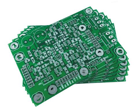
What are PCBs?
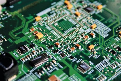
A Printed Circuit board (PCB) is a flat, typically rectangular, board made of insulating materials such as fiberglass or plastic, with conductive pathways etched or printed onto its surface. These conductive pathways, called traces, connect various electronic components like resistors, capacitors, and integrated circuits (ICs) to form a complete electrical circuit.
PCBs provide a stable and compact platform for electronic components, ensuring reliable connections and minimizing the risk of short circuits or other electrical issues. They also allow for the mass production of electronic devices, as the layout and design can be easily replicated across multiple boards.
History of PCBs
The concept of PCBs dates back to the early 20th century when inventors began experimenting with methods to create electrical connections on insulating materials. In 1925, Charles Ducas filed a patent for a method of creating an electrical path directly on an insulated surface by printing through a stencil with electrically conductive inks.
However, it wasn’t until after World War II that PCBs began to gain widespread adoption. In the 1940s, Paul Eisler, an Austrian engineer, developed a method for etching conductive pathways onto a non-conductive substrate, which laid the groundwork for modern PCB manufacturing.
As electronic devices became more complex and compact, PCBs evolved to meet the growing demands. In the 1960s, multi-layer PCBs were introduced, allowing for even greater circuit density and complexity. Today, PCBs can have up to 50 layers or more, depending on the application.
PCB Manufacturing Process
The manufacturing process for PCBs involves several steps, each requiring precision and attention to detail. The main stages of PCB manufacturing include:
-
Design: The PCB design is created using specialized software, such as Altium Designer or Eagle. The design includes the layout of the traces, the placement of components, and any necessary drill holes or cutouts.
-
Printing: The PCB design is printed onto a transparent film, which will be used to transfer the pattern onto the copper-clad board.
-
Etching: The copper-clad board is coated with a light-sensitive resist, and the transparent film with the PCB design is placed on top. The board is then exposed to UV light, hardening the resist where the traces will be. The unexposed resist is then removed, and the board is placed in an etching solution, which removes the unwanted copper, leaving only the traces behind.
-
Drilling: Holes are drilled into the board to accommodate through-hole components and provide connections between layers in multi-layer PCBs.
-
Plating: The holes are plated with a conductive material, typically copper, to ensure electrical connectivity between layers.
-
Solder Mask Application: A protective layer, called a solder mask, is applied to the board, covering the traces but leaving the pads and other areas that require soldering exposed.
-
Silkscreen: A silkscreen layer is added to the board, which includes text, logos, and other markings to assist in the assembly process and provide information about the board.
-
Surface Finish: A surface finish, such as HASL (Hot Air Solder Leveling) or ENIG (Electroless Nickel Immersion Gold), is applied to the exposed pads to prevent oxidation and improve solderability.
-
Electrical Testing: The completed PCB undergoes electrical testing to ensure that all connections are properly made and that there are no short circuits or other issues.
Types of PCBs
There are several types of PCBs, each with its own unique characteristics and applications. The most common types include:
-
Single-layer PCBs: These are the simplest and most cost-effective PCBs, with conductive traces on only one side of the board. They are suitable for basic, low-density circuits.
-
Double-layer PCBs: These PCBs have conductive traces on both sides of the board, allowing for more complex circuits and higher component density. They are commonly used in consumer electronics and industrial applications.
-
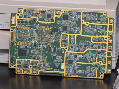
Multi-layer PCBs: These PCBs consist of three or more layers of conductive traces, separated by insulating layers. They offer the highest level of circuit density and are used in advanced applications such as aerospace, medical devices, and high-performance computing.
-
Flexible PCBs: These PCBs are made from flexible materials, such as polyimide, allowing them to bend and conform to various shapes. They are often used in wearable electronics, medical devices, and applications where space is limited.
-
Rigid-Flex PCBs: These PCBs combine the benefits of rigid and flexible PCBs, with rigid sections for mounting components and flexible sections for connecting different parts of the device. They are used in applications that require both stability and flexibility, such as automotive electronics and aerospace systems.

Applications of PCBs in Electrical Engineering
PCBs are used in virtually every aspect of electrical engineering, from consumer electronics to industrial control systems. Some of the most common applications include:
-
Consumer Electronics: PCBs are the backbone of modern consumer electronics, such as smartphones, tablets, laptops, and televisions. They enable the compact, high-performance designs that consumers have come to expect.
-
Automotive Electronics: PCBs are used extensively in automotive electronics, from engine control units and infotainment systems to advanced driver assistance systems (ADAS) and electric vehicle power management.
-
Industrial Control Systems: PCBs are essential components in industrial control systems, such as programmable logic controllers (PLCs), human-machine interfaces (HMIs), and supervisory control and data acquisition (SCADA) systems.
-
Medical Devices: PCBs are used in a wide range of medical devices, from patient monitoring systems and diagnostic equipment to implantable devices and wearable health monitors.
-
Aerospace and Defense: PCBs play a critical role in aerospace and defense applications, where reliability and performance are paramount. They are used in avionics systems, satellite communications, and military equipment.
-
Internet of Things (IoT): As the IoT continues to grow, PCBs are becoming increasingly important in the development of connected devices, sensors, and gateways that enable the collection and transmission of data.
Advantages of Using PCBs
PCBs offer numerous advantages over other methods of creating electrical circuits, such as point-to-point wiring or wire-wrap. Some of the key benefits include:
-
Reliability: PCBs provide a stable and reliable platform for electronic components, minimizing the risk of short circuits, loose connections, or other electrical issues.
-
Consistency: PCBs allow for the mass production of electronic devices with consistent quality and performance, as the layout and design can be easily replicated across multiple boards.
-
Compact Design: PCBs enable the creation of compact, high-density electronic devices, which is essential in today’s world of miniaturized electronics.
-
Cost-effective: Once the initial design and setup costs are covered, PCBs are relatively inexpensive to produce in large quantities, making them a cost-effective solution for mass-produced electronic devices.
-
Improved EMI/RFI Performance: Proper PCB design techniques, such as ground planes and controlled impedance traces, can help minimize electromagnetic interference (EMI) and radio-frequency interference (RFI), ensuring better overall system performance.
PCB Design Considerations
Designing a PCB requires careful consideration of various factors to ensure optimal performance, reliability, and manufacturability. Some of the key design considerations include:
-
Schematic Design: The first step in PCB design is creating a schematic that represents the electrical connections between components. This involves selecting the appropriate components, defining their values, and specifying their interconnections.
-
Component Placement: The placement of components on the PCB is critical for several reasons, including signal integrity, thermal management, and manufacturability. Components should be placed in a logical manner, with consideration for the flow of signals and the ease of assembly.
-
Trace Routing: The layout of the conductive traces on the PCB must be carefully designed to ensure proper signal integrity, minimize crosstalk, and avoid electromagnetic interference. This involves selecting the appropriate trace widths, spacing, and routing techniques, such as microstrip or stripline.
-
Power and Ground Distribution: Proper power and ground distribution is essential for the stable operation of electronic circuits. This involves creating low-impedance power and ground planes, using decoupling capacitors to minimize noise, and ensuring adequate current-carrying capacity for the traces.
-
Thermal Management: As electronic components generate heat during operation, it is important to design the PCB with thermal management in mind. This may involve the use of heat sinks, thermal vias, or other techniques to dissipate heat and prevent components from overheating.
-
Manufacturing Considerations: The PCB design must also take into account the limitations and requirements of the manufacturing process. This includes specifying the appropriate board material, layer stackup, and design rules, such as minimum trace widths and clearances.
PCB Testing and Inspection
Once a PCB has been manufactured, it must undergo thorough testing and inspection to ensure that it meets the required specifications and performs as intended. Some of the common testing and inspection methods include:
-
Visual Inspection: A visual inspection of the PCB is performed to check for any obvious defects, such as missing components, solder bridges, or damaged traces.
-
Automated Optical Inspection (AOI): AOI systems use cameras and image processing software to automatically detect and identify defects on the PCB, such as missing or misaligned components, solder issues, or trace defects.
-
X-ray Inspection: X-ray inspection is used to examine the internal structure of the PCB, particularly for multi-layer boards or components with hidden solder joints, such as ball grid arrays (BGAs).
-
In-Circuit Testing (ICT): ICT involves using a specialized test fixture to make electrical contact with the PCB and verify the presence, orientation, and value of each component, as well as the integrity of the interconnections between them.
-
Functional Testing: Functional testing involves powering up the PCB and verifying that it performs the intended functions correctly. This may involve the use of test software, signal generators, and oscilloscopes to analyze the board’s behavior.
Future Trends in PCB Technology
As electronic devices continue to evolve and become more complex, PCB technology must also advance to keep pace. Some of the future trends in PCB technology include:
-
High-Density Interconnect (HDI): HDI PCBs feature finer traces, smaller vias, and higher component density than traditional PCBs, enabling the creation of even more compact and complex electronic devices.
-
Embedded Components: Embedding components, such as resistors, capacitors, and ICs, within the layers of the PCB can further increase circuit density and reduce the overall size of electronic devices.
-
3D Printing: Advancements in 3D printing technology may enable the rapid prototyping and production of PCBs, allowing for greater design flexibility and faster time-to-market.
-
Flexible and Stretchable Electronics: As wearable and implantable electronic devices become more prevalent, the demand for flexible and stretchable PCBs will increase. These PCBs can conform to the shape of the human body and withstand the stresses of movement and flexing.
-
Eco-Friendly Materials: There is a growing trend towards the use of eco-friendly, biodegradable, and recyclable materials in PCB manufacturing, driven by concerns about electronic waste and environmental sustainability.
Frequently Asked Questions (FAQ)
-
What is the difference between a PCB and a breadboard?
A PCB is a permanent, custom-designed board with etched conductive traces that connect electronic components. A breadboard, on the other hand, is a temporary prototyping tool that allows components to be easily inserted and removed for testing and experimentation. -
Can PCBs be repaired if they are damaged?
In some cases, PCBs can be repaired if the damage is minor, such as a broken trace or a lifted pad. However, more extensive damage, such as delamination or severe overheating, may render the PCB irreparable, requiring replacement. -
What is the typical turnaround time for PCB manufacturing?
The turnaround time for PCB manufacturing varies depending on the complexity of the design, the chosen manufacturing options, and the workload of the fabrication house. Simple, two-layer PCBs can often be manufactured within a few days, while complex, multi-layer boards may take several weeks. -
How do I choose the right PCB manufacturer for my project?
When selecting a PCB manufacturer, consider factors such as their experience, capabilities, quality control processes, and customer support. Look for manufacturers with a proven track record in your industry, and be sure to request quotes from multiple sources to compare prices and lead times. -
What are the most common PCB design mistakes to avoid?
Some of the most common PCB design mistakes include incorrect component footprints, improper trace width and spacing, lack of proper grounding and power distribution, and failure to consider manufacturability constraints. To avoid these mistakes, use trusted component libraries, follow established design guidelines, and collaborate closely with your manufacturer throughout the design process.
Conclusion
PCBs are the foundation of modern electronics, enabling the creation of compact, reliable, and high-performance devices across a wide range of industries. From consumer gadgets to advanced aerospace systems, PCBs play a critical role in bringing electronic designs to life.
As an electrical engineer, understanding the fundamentals of PCBs, including their design, manufacturing, and testing processes, is essential for creating successful electronic products. By staying up-to-date with the latest trends and technologies in PCB development, engineers can continue to push the boundaries of what is possible in the world of electronics.
| PCB Type | Layers | Typical Applications |
|---|---|---|
| Single-layer PCB | 1 | Simple, low-density circuits |
| Double-layer PCB | 2 | Consumer electronics, industrial applications |
| Multi-layer PCB | 3+ | Advanced applications (aerospace, medical, etc.) |
| Flexible PCB | 1+ | Wearable electronics, medical devices, tight spaces |
| Rigid-Flex PCB | 1+ | Applications requiring both stability and flexibility |
In conclusion, PCBs are a vital component in electrical engineering, and their importance will only continue to grow as electronic devices become more advanced and ubiquitous. By mastering the art and science of PCB design and manufacturing, electrical engineers can create innovative solutions that shape the future of technology.
Leave a Reply