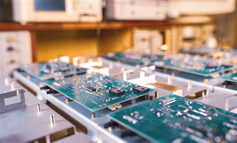
PCB Manufacturing: An Overview
PCB manufacturing is a complex process that requires precision, expertise, and state-of-the-art equipment. The main steps in PCB manufacturing include:
- Design and Layout
- Printing and Etching
- Drilling
- Plating
- Solder Mask Application
- Silkscreen Printing
- Surface Finish Application
- Electrical Testing
- Cutting and Packaging
Step 1: Design and Layout
The PCB manufacturing process begins with the design and layout of the Circuit Board. This step involves using specialized software, such as Altium Designer, Eagle, or KiCad, to create a digital representation of the PCB.
The design process includes:
- Schematic Capture: Creating a diagram that represents the electrical connections between components.
- Component Placement: Arranging the components on the board for optimal performance and manufacturability.
- Routing: Connecting the components with traces (copper paths) while adhering to design rules and constraints.
- Design Rule Check (DRC): Verifying that the design meets the manufacturer’s specifications and industry standards.
Once the design is complete, the files are sent to the PCB manufacturer in the form of Gerber files, which contain all the necessary information for fabrication.
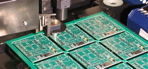
Step 2: Printing and Etching
The next step in the PCB manufacturing process is printing and etching the circuit pattern onto the copper-clad substrate. This is typically done using a photolithography process.
- Copper-clad Substrate Preparation: The substrate, usually made of fiberglass (FR4) or other materials, is cleaned and coated with a layer of photoresist, a light-sensitive material.
- Printing: The circuit pattern is printed onto a transparent film, called a photomask, which is then placed on top of the photoresist-coated substrate.
- Exposure: The substrate is exposed to UV light, which passes through the transparent areas of the photomask and hardens the photoresist in those areas.
- Developing: The unexposed photoresist is removed using a chemical developer, leaving behind the hardened photoresist that protects the copper underneath.
- Etching: The exposed copper is removed using an etchant solution, typically ammonium persulfate or ferric chloride, leaving only the copper traces protected by the hardened photoresist.
- Stripping: The remaining photoresist is stripped away, revealing the copper circuit pattern.
Step 3: Drilling
After the circuit pattern is etched, the PCB needs to be drilled to create holes for component leads and vias (connections between layers). This is done using computer-controlled drill machines, which can create holes as small as 0.1mm in diameter with high precision.
- Drill File Generation: The drill file, containing information about the size and location of each hole, is created from the PCB design software.
- Drilling: The PCB is placed in the drill machine, which uses the drill file to guide the high-speed drill bits through the board.
- Deburring: After drilling, the holes are deburred to remove any rough edges or debris that could affect the electrical connections.
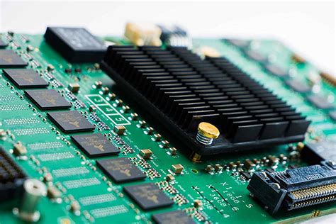
Step 4: Plating
To ensure reliable electrical connections and protect the copper traces from oxidation, the PCB undergoes a plating process. This involves coating the holes and traces with a thin layer of conductive material, typically copper.
- Desmear: The drilled holes are cleaned using a chemical or plasma process to remove any resin smear that may have formed during drilling.
- Electroless Copper Deposition: A thin layer of copper is deposited onto the holes and traces using an electroless plating process, which does not require an external electrical current.
- Electrolytic Copper Plating: A thicker layer of copper is deposited using an electrolytic plating process, which involves passing an electrical current through the board while it is immersed in a copper sulfate solution.
Step 5: Solder Mask Application
The solder mask is a protective layer applied to the PCB to prevent accidental short circuits and protect the copper traces from oxidation and environmental damage.
- Solder Mask Application: A liquid photoimageable solder mask ink is applied to both sides of the PCB using a screen printing or spraying process.
- Exposure: The solder mask is exposed to UV light through a photomask, which hardens the exposed areas.
- Developing: The unexposed solder mask is removed using a chemical developer, leaving behind the hardened solder mask that protects the copper traces.
- Curing: The solder mask is cured using heat to improve its durability and adhesion to the board.
Step 6: Silkscreen Printing
Silkscreen printing is used to add text, logos, and component identifiers to the PCB. This helps with assembly and troubleshooting.
- Silkscreen Ink Application: A silkscreen stencil is created with the desired artwork, and the ink is applied to the PCB through the stencil using a squeegee.
- Curing: The silkscreen ink is cured using heat or UV light to ensure its durability.
Step 7: Surface Finish Application
The surface finish is a protective layer applied to the exposed copper areas of the PCB to prevent oxidation and improve solderability. Common surface finishes include:
- Hot Air Solder Leveling (HASL)
- Organic Solderability Preservative (OSP)
- Electroless Nickel Immersion Gold (ENIG)
- Immersion Silver
- Immersion Tin
The choice of surface finish depends on the specific requirements of the PCB, such as the components used, the assembly process, and the operating environment.
Step 8: Electrical Testing
After the PCB has undergone all the fabrication steps, it is subjected to rigorous electrical testing to ensure its functionality and reliability.
- Flying Probe Test: A flying probe tester uses moving probes to test the continuity and isolation of the PCB traces and components.
- In-Circuit Test (ICT): An ICT fixture is used to test the PCB by applying electrical signals to specific points and measuring the response.
- Functional Test: The PCB is powered up and tested under real-world conditions to verify its performance and identify any issues.
Step 9: Cutting and Packaging
The final step in the PCB manufacturing process is cutting the panels into individual boards and packaging them for shipment.
- Depaneling: The PCB panels are cut into individual boards using a routing machine or a laser cutter.
- Packaging: The individual PCBs are inspected, cleaned, and packaged in ESD-safe bags or boxes for shipment to the customer.
PCB Manufacturing Technologies
Several technologies are used throughout the PCB manufacturing process to ensure high-quality, reliable boards. Some of these technologies include:
High-Density Interconnect (HDI)
HDI PCBs use advanced fabrication techniques to create smaller vias and finer traces, enabling higher component density and improved signal integrity.
Multilayer PCBs
Multilayer PCBs consist of multiple layers of copper traces and insulating material, allowing for more complex designs and higher component density.
Flexible PCBs
Flexible PCBs use flexible substrates, such as polyimide, to create bendable and conformable circuits for applications that require flexibility or space-saving designs.
Rigid-Flex PCBs
Rigid-flex PCBs combine rigid and flexible sections, offering the benefits of both technologies in a single board.
Frequently Asked Questions (FAQ)
-
What is the typical turnaround time for PCB manufacturing?
The turnaround time for PCB manufacturing depends on the complexity of the design, the number of layers, and the manufacturer’s workload. Typical turnaround times range from 1-2 weeks for simple designs to 4-6 weeks for complex, multilayer boards. -
What factors affect the cost of PCB manufacturing?
Several factors influence the cost of PCB manufacturing, including: - Board size and thickness
- Number of layers
- Material type (e.g., FR4, high-frequency laminates)
- Surface finish
- Quantity ordered
-
Design complexity (e.g., HDI, blind and buried vias)
-
What is the minimum feature size achievable in PCB manufacturing?
The minimum feature size depends on the manufacturer’s capabilities and the specific fabrication process used. Typical minimum feature sizes are: - Trace width: 0.1mm (4 mil)
- Trace spacing: 0.1mm (4 mil)
- Via diameter: 0.2mm (8 mil)
-
Hole size: 0.1mm (4 mil)
-
What file formats are used for PCB manufacturing?
The most common file formats used for PCB manufacturing are Gerber files (RS-274X) and Excellon drill files. These files contain all the necessary information for fabricating the PCB, including the copper layers, solder mask, silkscreen, and drill data. -
What quality control measures are used in PCB manufacturing?
PCB manufacturers employ various quality control measures to ensure the reliability and consistency of their products. These measures include: - Automated optical inspection (AOI)
- X-ray inspection
- Electrical testing (e.g., flying probe, ICT, functional testing)
- Cross-section analysis
- Thermal stress testing
- Visual inspection
| PCB Manufacturing Step | Description |
|---|---|
| Design and Layout | Creating a digital representation of the PCB using specialized software |
| Printing and Etching | Transferring the circuit pattern onto the copper-clad substrate using photolithography |
| Drilling | Creating holes for component leads and vias using computer-controlled drill machines |
| Plating | Coating the holes and traces with a thin layer of conductive material (typically copper) |
| Solder Mask Application | Applying a protective layer to prevent short circuits and protect the copper traces |
| Silkscreen Printing | Adding text, logos, and component identifiers to the PCB |
| Surface Finish Application | Applying a protective layer to the exposed copper areas to prevent oxidation and improve solderability |
| Electrical Testing | Verifying the functionality and reliability of the PCB through various testing methods |
| Cutting and Packaging | Cutting the panels into individual boards and packaging them for shipment |

Conclusion
PCB manufacturing is a complex, multi-step process that requires precision, expertise, and advanced technologies. By understanding the steps involved in PCB manufacturing, from design and layout to cutting and packaging, designers and engineers can create high-quality, reliable circuit boards that meet the demands of modern electronic devices. As technology continues to evolve, PCB manufacturing processes will adapt to support increasingly complex designs and applications.
Leave a Reply