Introduction to PCBs
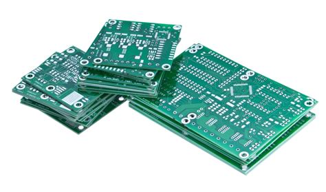
PCB stands for “printed Circuit Board”. PCBs are thin boards made of fiberglass or composite material that have conductive pathways printed or etched onto them to connect electronic components. They are found in virtually every electronic device, from simple toys and appliances to complex computers and medical equipment.
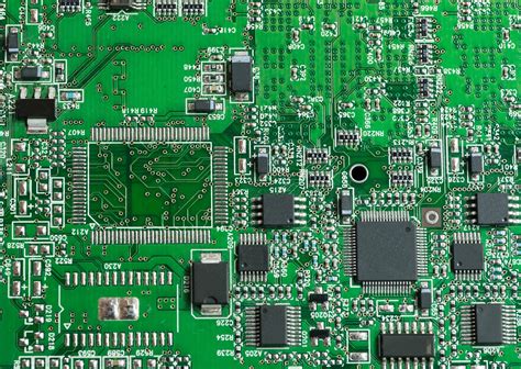
PCBs allow electronic circuits to be manufactured in a standardized, automated way. Components like resistors, capacitors, and integrated circuits are soldered onto the conductive traces of the PCB to create a complete circuit. PCBs mechanically support and electrically connect the electronic components using conductive tracks, pads and other features etched from copper sheets laminated onto a non-conductive substrate.
History of PCBs
The concept of printed circuits originated in the early 20th century, but the modern PCB as we know it today was invented in the 1940s. During World War II, the U.S. military began using PCBs in proximity fuzes for artillery shells, which required a small, rugged and mass-producible circuit. In 1947, American engineer Paul Eisler developed the first method for etching circuit patterns onto a layer of copper foil bonded to a non-conductive glass-reinforced epoxy resin board.
Throughout the 1950s and 60s, PCB manufacturing techniques advanced rapidly as the electronics industry grew. Silk screen printing of circuit patterns, soldering methods, multilayer PCBs, and surface-mount technology were developed and refined. By the 1980s, computer-aided design (CAD) software and numerically-controlled machines made PCB Design and manufacturing faster and more precise than ever before.
How Are PCBs Made?
The PCB manufacturing process typically involves the following steps:
-
Design: The circuit schematic and board layout are designed using CAD software. The designer determines the size and shape of the board, placement of components, and routing of conductive traces.
-
Printing: The circuit design is printed onto a transparent film or photomask. For multilayer boards, a separate film is made for each layer.
-
Etching: Copper-clad sheets of insulating material (substrate) are coated with a light-sensitive resist. The photomask is placed on top and exposed to light, hardening the unmasked areas. The board is then chemically etched to remove the unhardened resist and unwanted copper, leaving only the desired circuit pattern.
-
Drilling: Holes are drilled through the board to accommodate through-hole components or to create vias that connect different layers.
-
Plating: The holes are plated with copper to create electrical connections between layers. A thin layer of soldermask is applied to the board to insulate and protect the copper traces.
-
Silkscreening: Text and symbols are silkscreened onto the board to label components and test points.
-
Finishing: The PCB is cut and shaped to its final form factor. Surface finishes like gold, silver or lead-free HASL are applied to protect the copper and facilitate soldering.
-
Assembly: Components are placed and soldered onto the board using automated pick-and-place machines and reflow ovens. The assembled PCB is then tested and inspected for quality control.
PCB Substrates and Materials
PCBs are made from a variety of materials depending on the intended application and required properties such as durability, thermal conductivity, dielectric constant, and cost. The most common PCB substrates are:
| Material | Composition | Properties | Typical Uses |
|---|---|---|---|
| FR-4 | Fiberglass-reinforced epoxy | Good insulation, mechanical strength, flame resistance | General purpose, consumer electronics |
| Alumina | Aluminum oxide ceramic | High thermal conductivity, stability at high temperatures | High-power LEDs, automotive, aerospace |
| Polyimide | High-temperature thermoplastic | Flexible, lightweight, resistant to heat and chemicals | Wearables, aerospace, medical devices |
| PTFE | Polytetrafluoroethylene (Teflon) | Low dielectric constant, low dissipation factor | RF/microwave circuits, radar, telecommunications |
| Metal core | Aluminum or copper base with thin dielectric layer | Excellent thermal conductivity | Power electronics, LED lighting |
The conductive traces on a PCB are usually made of copper, which has high electrical conductivity and is relatively inexpensive. The copper foil is laminated onto the substrate using heat and adhesives. Copper thickness is measured in ounces per square foot, with 1 oz/ft² (35 µm) being the most common. Thicker copper is used for high-current applications or to improve mechanical stability.
Types of PCBs
PCBs come in several different varieties depending on the number of conductive layers, materials used, and special features. The most common types are:
Single-layer PCBs
Single-layer or single-sided PCBs have conductive traces on only one side of the substrate. They are the simplest and cheapest type of PCB, but are limited in circuit complexity and density. Single-layer PCBs are used for basic electronic devices like power supplies, LED lights, and toys.
Double-layer PCBs
Double-layer or double-sided PCBs have conductive traces on both sides of the substrate. The two layers are connected by vias, which are small plated holes that allow signals to pass through the board. Double-layer PCBs offer more flexibility in circuit design and higher component density than single-layer boards. They are used in a wide range of applications, from consumer electronics to industrial controls.
Multilayer PCBs
Multilayer PCBs have three or more conductive layers separated by insulating material. The layers are interconnected by vias that can be drilled through the entire board (through holes) or only partway (blind or buried vias). Multilayer PCBs allow for highly complex circuits with high component density and signal integrity. They are used in advanced electronic devices like smartphones, computers, and medical equipment.
| Layers | Typical Thickness (mm) | Common Uses |
|---|---|---|
| 4 | 1.0 – 1.6 | Consumer electronics, automotive, industrial controls |
| 6 | 1.2 – 2.4 | Telecommunications, aerospace, defense |
| 8 | 1.6 – 2.8 | High-speed digital devices, servers, datacenters |
| 10+ | 2.0 – 3.2 | Supercomputers, satellites, medical imaging equipment |
Flexible PCBs
Flexible or flex PCBs are made from thin, flexible materials like polyimide or PEEK. They can be bent, twisted, or folded to fit into tight spaces or conform to curved surfaces. Flex PCBs are often used in wearable devices, medical implants, and aerospace applications where traditional rigid PCBs are not suitable.
Rigid-flex PCBs
Rigid-flex PCBs combine rigid and flexible sections in a single board. The rigid sections provide mechanical support and stability, while the flexible sections allow the board to be bent or folded. Rigid-flex PCBs are used in applications that require both high component density and flexibility, such as cameras, printers, and automotive electronics.

PCB Design Considerations
Designing a PCB involves balancing many factors to create a functional, reliable, and manufacturable board. Some key considerations include:
Schematic capture
The first step in PCB design is creating a schematic diagram that shows the electrical connections between components. This is typically done using electronic design automation (EDA) software like KiCad, Eagle, or Altium Designer. The schematic captures the logical design of the circuit and serves as a blueprint for the physical board layout.
Component selection and placement
Components must be carefully selected based on their electrical specifications, package type, and availability. Designers must also consider factors like power dissipation, thermal management, and electromagnetic interference (EMI) when choosing components.
Component placement on the board is critical for signal integrity, manufacturability, and ease of assembly. Components should be grouped logically and placed to minimize the length of traces and the number of vias. Designers must also follow design rules for minimum spacing between components and traces to avoid short circuits and EMI.
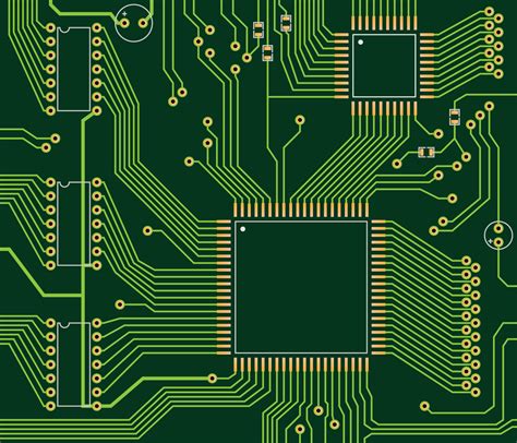
Routing and trace design
The next step is routing the conductive traces between components according to the schematic. Traces must be sized appropriately for the expected current and voltage levels to avoid overheating or signal loss. Trace width, spacing, and geometry also affect the impedance and propagation delay of high-speed signals.
Designers must also consider the number of layers needed to route all the connections while minimizing board size and complexity. Multilayer boards allow for more routing flexibility but are more expensive to manufacture.
Stackup and materials
The choice of substrate material and the arrangement of conductive and insulating layers (stackup) are critical for the electrical and mechanical performance of the PCB. Factors like dielectric constant, loss tangent, and thermal conductivity must be considered based on the operating frequency, power level, and environmental conditions of the circuit.
Common stackups for multilayer PCBs include:
| Layer | 4-layer | 6-layer | 8-layer |
|---|---|---|---|
| Top | Signal | Signal | Signal |
| 2 | Ground | Ground | Ground |
| 3 | Power | Signal | Signal |
| 4 | Signal | Power | Power |
| 5 | Ground | Ground | |
| 6 | Signal | Signal | |
| 7 | Power | ||
| Bottom | Signal |
Design rule checking (DRC)
Before sending a PCB design to manufacturing, it must be checked against a set of design rules to ensure that it meets the fabricator’s capabilities and quality standards. DRC software checks for errors like trace width and spacing violations, missing or overlapping vias, and component clearance issues. DRC helps to catch mistakes early and avoid costly redesigns or manufacturing defects.
PCB Assembly Techniques
Once a PCB is fabricated, the components must be assembled onto the board to create a functional circuit. The two main assembly techniques are:
Through-hole assembly
Through-hole components have long leads that are inserted into holes drilled through the PCB and soldered to pads on the opposite side. Through-hole assembly is simple and reliable but requires more manual labor and takes up more space than surface-mount assembly.
Surface-mount assembly
Surface-mount components have small metal pads or leads that are soldered directly onto pads on the surface of the PCB. Surface-mount assembly allows for smaller components and higher density than through-hole assembly, but requires more precise manufacturing and placement equipment.
Most modern PCBs use a combination of through-hole and surface-mount components to balance cost, density, and reliability. The choice of assembly technique depends on factors like the component types, board size and complexity, and production volume.
PCB Testing and Quality Control
Thorough testing and quality control are essential to ensure that PCBs function correctly and reliably. Some common testing methods include:
Visual inspection
PCBs are visually inspected for defects like missing or misaligned components, solder bridges, and damaged traces. Automated optical inspection (AOI) systems can quickly scan boards and compare them to a reference image to detect errors.
Electrical testing
PCBs are powered on and tested for proper functionality using oscilloscopes, multimeters, and other test equipment. In-circuit testing (ICT) involves probing individual components and nets to verify their values and connections. Flying probe testing uses moving probes to test different points on the board without the need for a custom fixture.
Environmental testing
PCBs may be subjected to environmental stresses like temperature cycling, humidity, vibration, and shock to simulate real-world operating conditions. These tests help to identify design weaknesses and potential failure modes.
Burn-in testing
PCBs are operated at elevated temperatures and voltages for an extended period of time to identify early failures and infant mortality issues. Burn-in testing helps to weed out defective boards before they are shipped to customers.
Functional testing
PCBs are integrated into the final product or system and tested for proper operation under normal and extreme conditions. Functional testing verifies that the board meets all performance and reliability requirements.
PCB Standards and Regulations
PCBs must comply with various industry standards and government regulations to ensure safety, reliability, and compatibility. Some important standards include:
IPC standards
The Association Connecting Electronics Industries (IPC) publishes a wide range of standards for PCB design, fabrication, assembly, and testing. Some key standards are:
- IPC-2221: Generic Standard on Printed Board Design
- IPC-6012: Qualification and Performance Specification for Rigid Printed Boards
- IPC-A-600: Acceptability of Printed Boards
- IPC-A-610: Acceptability of Electronic Assemblies
- IPC-7711/7721: Rework, Modification and Repair of Electronic Assemblies
UL standards
Underwriters Laboratories (UL) is a global safety certification company that tests and certifies PCBs and electronic equipment. UL standards cover areas like flammability, electrical safety, and environmental resistance. Some relevant standards are:
- UL 94: Standard for Safety of Flammability of Plastic Materials for Parts in Devices and Appliances
- UL 796: Standard for Safety of Printed-Wiring Boards
- UL 840: Standard for Safety of Insulation Coordination Including Clearances and Creepage Distances for Electrical Equipment
RoHS and REACH directives
The Restriction of Hazardous Substances (RoHS) and Registration, Evaluation, Authorization and Restriction of Chemicals (REACH) are European Union directives that restrict the use of certain hazardous substances in electronic equipment. PCBs must comply with these directives to be sold in the EU market.
Frequently Asked Questions (FAQ)
What is the difference between a PCB and a PCBA?
A PCB is a bare board with no components attached, while a PCBA (Printed Circuit Board assembly) is a board with components soldered onto it. PCBs are the raw material for PCBAs, which are the functional building blocks of electronic devices.
How much does it cost to manufacture a PCB?
The cost of manufacturing a PCB depends on many factors, including the size, complexity, materials, and quantity of boards ordered. Simple, single-layer PCBs can cost less than $1 per board in large quantities, while complex, multilayer boards can cost hundreds of dollars each. Setup and tooling charges also add to the total cost, especially for small production runs.
What is the typical turnaround time for PCB manufacturing?
Turnaround time for PCB manufacturing varies depending on the complexity of the board, the fabricator’s workload, and the shipping method. Simple, quick-turn PCBs can be manufactured and shipped within 24-48 hours, while complex, high-reliability boards may take several weeks. Most PCB fabricators offer standard lead times of 1-2 weeks for prototype quantities and 3-4 weeks for production quantities.
What software is used for PCB design?
There are many different software tools used for PCB design, ranging from simple, free programs to complex, professional-grade suites. Some popular PCB design software includes:
- KiCad (free and open-source)
- EAGLE (low-cost, widely used by hobbyists and small businesses)
- Altium Designer (professional-grade, used by large companies and high-end designs)
- OrCAD (professional-grade, part of Cadence Design Systems)
- Mentor Graphics PADS (professional-grade, part of Siemens EDA)
The choice of software depends on factors like design complexity, team size, budget, and compatibility with other tools and processes.
Can PCBs be recycled?
Yes, PCBs can be recycled to recover valuable materials like copper, gold, and palladium. However, the recycling process is complex and expensive due to the need to separate the metals from the non-conductive substrates and remove hazardous substances like lead and brominated flame retardants.
The recycling process typically involves shredding the PCBs, separating the metals with magnets or eddy currents, and refining the metals through smelting or chemical processes. The remaining non-metallic fraction can be used as a filler material in construction or landfilled.
Recycling PCBs helps to conserve natural resources, reduce electronic waste, and prevent toxic substances from entering the environment. However, the economics of PCB recycling are challenging due to the low value of the recovered materials relative to the cost of collection, processing, and transportation.
Conclusion
PCBs are the backbone of modern electronics, enabling the creation of complex, reliable, and affordable devices that have transformed every aspect of our lives. From simple single-layer boards to advanced multilayer assemblies, PCBs have evolved to meet the ever-increasing demands of the electronics industry.
Designing and manufacturing PCBs requires a deep understanding of electrical engineering, materials science, and manufacturing processes. PCB designers must balance many competing factors to create boards that are functional, reliable, and cost-effective.
As electronic devices continue to become smaller, faster, and more powerful, PCBs will play an even greater role in enabling new technologies and applications. Innovations in materials, manufacturing, and design tools will help to push the boundaries of what is possible with PCBs and open up new frontiers in electronics.
Leave a Reply