Introduction to PCB Functionality
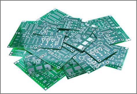
A Printed Circuit Board (PCB) is a fundamental component in modern electronics. It is a thin board made of fiberglass or other composite material, with conductive pathways etched or printed onto its surface. These pathways, known as traces, connect various electronic components such as resistors, capacitors, and integrated circuits (ICs) to create a functional electronic device. In this article, we will delve into the intricacies of PCB Functionality, exploring how these essential components work together to bring electronic devices to life.
The Composition of a PCB
Substrate Material
The base material of a PCB is called the substrate. It is typically made of a non-conductive material such as fiberglass, epoxy, or other composite materials. The substrate provides a sturdy foundation for the conductive traces and electronic components. Some common substrate materials include:
| Material | Description | Advantages |
|---|---|---|
| FR-4 | Fiberglass-reinforced epoxy laminate | High strength, good insulation properties |
| CEM-1 | Composite epoxy material | Lower cost than FR-4, suitable for less demanding applications |
| Polyimide | High-temperature resistant polymer | Excellent thermal stability, used in high-temperature applications |
Copper Traces
Conductive pathways, known as traces, are etched or printed onto the surface of the substrate. These traces are typically made of copper due to its excellent electrical conductivity and relatively low cost. The thickness and width of the traces depend on the current-carrying requirements of the circuit. Thicker traces are used for high-current applications, while thinner traces are suitable for low-current signals.
Solder Mask
A solder mask is a thin layer of polymer applied over the copper traces, leaving only the exposed areas where components will be soldered. The solder mask serves several purposes:
- Insulation: It prevents accidental short circuits between adjacent traces.
- Protection: The solder mask protects the copper traces from oxidation and other environmental factors.
- Aesthetics: Solder masks are available in various colors, allowing for better visual identification of components and improved aesthetics.
Silkscreen
The silkscreen is a printed layer on top of the solder mask that provides text, symbols, and logos for easy identification of components and their placement. It helps during the assembly process and makes it easier to debug and repair the PCB if needed.
PCB Manufacturing Process
The manufacturing process of a PCB involves several steps, each crucial to ensuring the proper functionality and reliability of the final product.
Design and Layout
The first step in PCB manufacturing is designing the circuit schematic and creating the PCB layout using specialized software. The layout determines the placement of components and the routing of traces. Designers must adhere to design rules and guidelines to ensure proper functionality and manufacturability.
Printing and Etching
Once the design is finalized, the PCB layout is printed onto a photosensitive film or directly onto the copper-clad substrate. The exposed areas of the copper are then etched away using a chemical process, leaving only the desired traces.
Drilling and Plating
Holes are drilled through the PCB to accommodate through-hole components and provide interconnections between layers in multi-layer boards. The holes are then plated with copper to ensure electrical continuity.
Solder Mask and Silkscreen Application
The solder mask is applied to the PCB, covering the copper traces while leaving the component pads exposed. The silkscreen is then printed on top of the solder mask, providing the necessary labels and markings.
Component Assembly
Finally, the electronic components are soldered onto the PCB, either through manual hand soldering or automated processes such as wave soldering or reflow soldering.

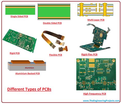
Types of PCBs
There are several types of PCBs, each with its own unique characteristics and applications.
Single-Layer PCBs
Single-layer PCBs have conductive traces on only one side of the substrate. They are the simplest and most cost-effective type of PCB, suitable for low-complexity circuits and prototyping.
Double-Layer PCBs
Double-layer PCBs have conductive traces on both sides of the substrate, allowing for more complex circuits and higher component density. The two layers are connected through plated through-holes (vias).
Multi-Layer PCBs
Multi-layer PCBs consist of three or more layers of conductive traces, separated by insulating layers. They offer the highest component density and are used in complex electronic devices such as smartphones, computers, and aerospace systems.
Flexible PCBs
Flexible PCBs are made using flexible substrate materials such as polyimide. They can bend and conform to various shapes, making them ideal for applications where space is limited or where the PCB needs to fit into a curved enclosure.
Rigid-Flex PCBs
Rigid-flex PCBs combine the benefits of both rigid and flexible PCBs. They consist of rigid sections connected by flexible sections, allowing for three-dimensional assembly and improved reliability in applications with frequent motion or vibration.
PCB Functionality in Electronic Devices
PCBs play a crucial role in the functionality of electronic devices, providing the necessary interconnections and support for electronic components.
Power Distribution
One of the primary functions of a PCB is to distribute power to the various components on the board. The PCB traces act as a network of power rails, delivering the required voltage and current to each component. Proper power distribution is essential for the stable operation of the electronic device.
Signal Routing
PCBs also facilitate the routing of signals between components. The conductive traces act as pathways for electrical signals, allowing communication between ICs, sensors, and other components. Proper signal routing is crucial for maintaining signal integrity and minimizing interference.
Component Mounting
PCBs provide a stable platform for mounting electronic components. Through-hole components are inserted into drilled holes and soldered in place, while surface-mount components are soldered directly onto the copper pads on the PCB surface. The PCB ensures proper positioning and mechanical support for the components.
Thermal Management
PCBs also play a role in thermal management, helping to dissipate heat generated by electronic components. Copper traces and planes can act as heat sinks, spreading the heat across the PCB surface. In some cases, additional thermal management techniques, such as heatsinks or fans, may be used in conjunction with the PCB to ensure proper cooling.
PCB Design Considerations
Designing a functional and reliable PCB requires careful consideration of several factors.
Component Placement
Proper component placement is essential for optimal PCB functionality. Components should be placed in a way that minimizes the length of traces, reduces interference, and facilitates efficient power distribution. Designers must also consider the mechanical constraints of the device and ensure adequate spacing between components.
Trace Width and Spacing
The width and spacing of traces on a PCB depend on the electrical requirements of the circuit. Wider traces are used for high-current paths, while narrower traces are suitable for low-current signals. Proper spacing between traces is necessary to prevent signal crosstalk and ensure the PCB meets the required electrical clearance and creepage distances.
Grounding and Shielding
Proper grounding and shielding techniques are crucial for minimizing electromagnetic interference (EMI) and ensuring the stable operation of the electronic device. Ground planes, which are large areas of copper connected to the ground potential, help to provide a low-impedance return path for currents and shield sensitive signals from interference.
Manufacturability
PCB designers must also consider the manufacturability of the board. This includes adhering to design rules and guidelines set by the PCB manufacturer, such as minimum trace widths, hole sizes, and clearances. Designing for manufacturability helps to ensure the PCB can be reliably produced and reduces the risk of defects.
FAQ
-
What is the difference between a through-hole and surface-mount PCB?
Through-hole PCBs have components with long leads that are inserted into drilled holes and soldered on the opposite side of the board. Surface-mount PCBs have components that are soldered directly onto the copper pads on the surface of the board. Surface-mount technology allows for higher component density and smaller board sizes. -
Can a PCB be repaired if damaged?
In many cases, PCBs can be repaired if the damage is not too extensive. Common repairs include replacing damaged components, repairing broken traces, and adding jumper wires to bypass damaged areas. However, the feasibility of repair depends on the complexity of the PCB and the extent of the damage. -
What is the purpose of vias in a PCB?
Vias are small holes drilled through a PCB that allow electrical connections between different layers of the board. They are used to route signals and power between layers, enabling more complex circuits and higher component density. -
How important is the choice of substrate material in PCB design?
The choice of substrate material is crucial in PCB design, as it affects the board’s mechanical strength, thermal stability, and dielectric properties. The substrate must be able to withstand the environmental conditions and mechanical stresses the PCB will be subjected to in its intended application. -
What is the role of solder paste in PCB assembly?
Solder paste is a mixture of tiny solder particles suspended in a flux medium. It is applied to the component pads on the PCB before the components are placed. During the soldering process, the solder paste melts, forming a strong electrical and mechanical connection between the components and the PCB.
Conclusion
PCBs are the backbone of modern electronics, providing the necessary interconnections and support for electronic components. By understanding how PCBs work and the various factors that influence their functionality, designers and engineers can create reliable and efficient electronic devices. From the composition of the board to the manufacturing process and design considerations, each aspect of a PCB plays a crucial role in ensuring the proper operation of the final product. As technology continues to advance, PCBs will remain an essential component in the ever-evolving world of electronics.
Leave a Reply