What is the Definition of PCB?
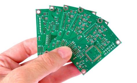
PCB stands for Printed Circuit Board. It is a thin board made of fiberglass or other composite material, with conductive pathways etched or printed onto the surface. These pathways, also known as traces, connect various electronic components such as resistors, capacitors, and integrated circuits to form a complete electronic circuit.
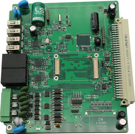
PCBs are used in almost all electronic devices, from simple consumer gadgets like calculators and remote controls to complex industrial equipment and aerospace systems. They provide a reliable and efficient means of interconnecting electronic components, while also providing mechanical support and protection.
History of PCBs
The concept of printed circuit boards dates back to the early 20th century. In 1903, Albert Hanson, a German inventor, filed a patent for a method of creating an electrical connection between layers of copper foil using a conductive ink. This laid the foundation for the development of modern PCBs.
In the 1920s, Charles Ducas, an American inventor, created a process for electroplating circuit patterns onto a board. This method was further refined by Paul Eisler, an Austrian engineer, who developed a process for etching copper foil to create circuit patterns in the 1930s.
During World War II, the demand for reliable and compact electronic equipment led to significant advancements in PCB technology. The United States National Bureau of Standards (now known as the National Institute of Standards and Technology) developed a process for printing circuit patterns onto a ceramic substrate, which was used in proximity fuzes for artillery shells.
After the war, the PCB industry continued to grow and evolve. In the 1950s, the introduction of through-hole technology allowed for the creation of double-sided PCBs, which greatly increased the density of components that could be placed on a single board. The 1960s saw the development of multilayer PCBs, which further increased component density and allowed for more complex circuits.
Today, PCBs are an essential part of the electronics industry, with advancements in materials, manufacturing processes, and design software enabling the creation of increasingly sophisticated and miniaturized electronic devices.
Types of PCBs
There are several types of PCBs, each with its own unique characteristics and applications. The most common types include:
-
Single-sided PCBs: These have conductive traces on only one side of the board. They are the simplest and most cost-effective type of PCB, suitable for low-complexity circuits.
-
Double-sided PCBs: These have conductive traces on both sides of the board, allowing for a higher component density and more complex circuits. The two sides are connected using through-hole technology.
-
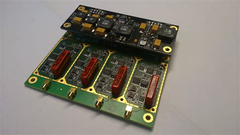
Multilayer PCBs: These consist of multiple layers of conductive traces separated by insulating layers. They can accommodate highly complex circuits and are used in applications where space is limited, such as smartphones and laptops.
-
Flexible PCBs: These are made from flexible materials, such as polyimide, allowing them to bend and conform to various shapes. They are used in applications where flexibility and durability are essential, such as wearable electronics and automotive systems.
-
Rigid-Flex PCBs: These are a combination of rigid and flexible PCBs, offering the benefits of both types. They are used in applications that require both stability and flexibility, such as aerospace and medical devices.
How are PCBs Manufactured?
The manufacturing process for PCBs involves several steps, each requiring precision and attention to detail. The main steps include:
-
Design: The PCB Design is created using specialized software, such as Eagle, KiCad, or Altium Designer. The design includes the placement of components, routing of traces, and creation of solder masks and silkscreens.
-
Printing: The designed circuit pattern is printed onto a photosensitive film or directly onto the copper-clad board using a plotter or laser printer.
-
Exposure: The photosensitive film or board is exposed to UV light, which hardens the areas not covered by the circuit pattern.
-
Developing: The exposed board is placed in a chemical bath, which removes the unhardened photoresist, leaving behind the circuit pattern.
-
Etching: The board is placed in an etchant solution, which removes the copper not protected by the hardened photoresist, creating the conductive traces.
-
Drilling: Holes are drilled through the board to accommodate through-hole components and provide connections between layers in multilayer PCBs.
-
Plating: A thin layer of copper is electroplated onto the board to provide a better surface for soldering and to protect the traces from oxidation.
-
Solder Mask and Silkscreen: A solder mask is applied to the board to protect the traces from short circuits and to prevent solder from bridging between pads. A silkscreen is then applied to provide component labels and other identifying markings.
-
Surface Finishing: A surface finish, such as HASL (Hot Air Solder Leveling), ENIG (Electroless Nickel Immersion Gold), or OSP (Organic Solderability Preservative), is applied to the board to improve solderability and protect the copper from oxidation.
-
Inspection and Testing: The completed PCB is inspected for defects and tested to ensure proper functionality.
| Step | Description |
|---|---|
| Design | PCB design created using specialized software |
| Printing | Circuit pattern printed onto photosensitive film or board |
| Exposure | Board exposed to UV light to harden photoresist |
| Developing | Unhardened photoresist removed in chemical bath |
| Etching | Copper not protected by photoresist removed to create traces |
| Drilling | Holes drilled for through-hole components and layer connections |
| Plating | Copper electroplated onto board for better soldering and protection |
| Solder Mask and Silkscreen | Solder mask and silkscreen applied for protection and identification |
| Surface Finishing | Surface finish applied to improve solderability and protect copper |
| Inspection and Testing | Completed PCB inspected and tested for functionality |
Advantages of Using PCBs
PCBs offer numerous advantages over other methods of interconnecting electronic components, such as point-to-point wiring or wire-wrap. Some of the key benefits include:
-
Reliability: PCBs provide a stable and reliable means of connecting components, reducing the risk of short circuits, loose connections, and other issues that can cause device failure.
-
Consistency: The automated manufacturing process ensures that each PCB is produced to the same specifications, minimizing variations in performance and quality.
-
Space Efficiency: PCBs allow for the dense packing of components, enabling the creation of compact and lightweight electronic devices.
-
Cost-Effectiveness: The automated manufacturing process and the ability to produce PCBs in large quantities make them a cost-effective solution for electronic device production.
-
Improved Signal Integrity: The precise layout and routing of traces on a PCB help to minimize signal interference and ensure proper signal timing, which is crucial for high-speed and high-frequency applications.
-
Simplified Assembly: PCBs provide a clear and organized layout for components, making the assembly process more efficient and less prone to errors.
-
Enhanced Heat Dissipation: PCBs can be designed with thermal management in mind, incorporating features such as heat sinks and thermal vias to dissipate heat generated by components.

Applications of PCBs
PCBs are used in a wide range of electronic devices and systems, spanning various industries and applications. Some common examples include:
-
Consumer Electronics: PCBs are found in smartphones, tablets, laptops, televisions, gaming consoles, and home appliances.
-
Automotive Electronics: Modern vehicles rely heavily on PCBs for various systems, such as engine control units, infotainment systems, and advanced driver assistance systems (ADAS).
-
Medical Devices: PCBs are used in a variety of medical devices, including patient monitors, imaging equipment, and implantable devices like pacemakers and insulin pumps.
-
Industrial Equipment: PCBs are essential components in industrial automation systems, process control equipment, and power electronics.
-
Aerospace and Defense: PCBs are used in avionics, satellite systems, radar equipment, and other critical aerospace and defense applications.
-
Telecommunications: PCBs are crucial for the functioning of network infrastructure, such as routers, switches, and base stations.
-
Internet of Things (IoT): The proliferation of connected devices in the IoT era has driven the demand for compact, low-power PCBs that can be integrated into sensors, wearables, and smart home devices.
Future Trends in PCB Technology
As electronic devices continue to evolve and new technologies emerge, the PCB industry must adapt to meet the changing demands. Some of the key trends shaping the future of PCB technology include:
-
Miniaturization: The ongoing trend towards smaller, more compact electronic devices is driving the development of advanced PCB manufacturing techniques, such as high-density interconnect (HDI) and embedded component technology.
-
Flexible and Stretchable PCBs: The growing demand for wearable electronics and flexible displays is fueling the development of flexible and stretchable PCBs that can conform to various shapes and withstand repeated bending and stretching.
-
3D Printing: Additive manufacturing techniques, such as 3D printing, are being explored as a means of creating complex, three-dimensional PCB structures that can accommodate more components in a smaller space.
-
Advanced Materials: Researchers are investigating new materials, such as graphene and carbon nanotubes, which offer superior electrical and thermal properties compared to traditional PCB materials.
-
Sustainable Manufacturing: As environmental concerns grow, the PCB industry is focusing on developing more sustainable manufacturing processes and materials, such as lead-free solders and halogen-free laminates.
-
Intelligent PCBs: The integration of sensors, microcontrollers, and other intelligent components directly onto PCBs is enabling the creation of smart, self-monitoring electronic systems.
-
High-Speed and High-Frequency: The demand for faster data transmission and higher bandwidth is driving the development of PCBs that can support high-speed and high-frequency signals, such as those used in 5G networks and high-performance computing applications.
Frequently Asked Questions (FAQ)
- What is the difference between a PCB and a PCBA?
-
A PCB is the bare board with the conductive traces and pads, while a PCBA (Printed Circuit Board Assembly) is a PCB with all the electronic components soldered onto it, forming a complete functional circuit.
-
How do I choose the right type of PCB for my project?
-
The choice of PCB type depends on factors such as the complexity of the circuit, the space available, the operating environment, and the budget. Consider the specific requirements of your project and consult with a PCB manufacturer or design expert to determine the most suitable type.
-
What is the typical turnaround time for PCB manufacturing?
-
The turnaround time for PCB manufacturing varies depending on the complexity of the design, the type of PCB, and the manufacturer. Simple, single-sided PCBs can be produced in a matter of days, while complex, multilayer PCBs may take several weeks. Rush services are often available for a premium.
-
How can I ensure the quality of my PCBs?
-
To ensure the quality of your PCBs, work with a reputable manufacturer that adheres to industry standards and has a proven track record. Provide clear and detailed design files, and communicate your requirements thoroughly. Consider having your PCBs inspected and tested by a third-party service before assembly.
-
What are some common PCB design mistakes to avoid?
- Some common PCB design mistakes include improper component placement, incorrect trace width and spacing, lack of proper grounding and shielding, and failure to account for thermal management. To avoid these mistakes, follow best practices for PCB design, use design rule checks (DRC) in your software, and have your designs reviewed by experienced engineers.
In conclusion, PCBs are the backbone of modern electronics, providing a reliable and efficient means of interconnecting components to create complex circuits. Understanding the basics of PCB technology, including the types, manufacturing process, and applications, is essential for anyone involved in the design, production, or use of electronic devices. As the demand for more advanced and miniaturized electronics continues to grow, the PCB industry will play a crucial role in shaping the future of technology.
Leave a Reply