Introduction to PCB
A Printed Circuit Board (PCB) is a fundamental component in modern electronic devices. It is a flat board made of insulating material, usually fiberglass or composite epoxy, with conductive copper traces printed on its surface. These traces connect various electronic components, such as resistors, capacitors, integrated circuits (ICs), and other elements, to create a complete electronic circuit.
PCBs have revolutionized the electronics industry by providing a reliable, compact, and cost-effective method of assembling electronic circuits. They are used in a wide range of applications, from simple consumer gadgets to complex industrial equipment, aerospace systems, and medical devices.
History of PCB
The concept of printed circuits dates back to the early 20th century. In 1903, Albert Hanson, a German inventor, filed a patent for a method of creating conductive patterns on an insulating substrate. However, it wasn’t until the 1940s that printed circuit boards began to gain widespread adoption.
During World War II, the United States military heavily invested in the development of PCB technology to improve the reliability and efficiency of their electronic equipment. In 1947, the U.S. Army Signal Corps released a report detailing the use of printed circuits in proximity fuzes for artillery shells, which greatly reduced the size and manufacturing time of these devices.
In the following decades, PCB technology continued to evolve. The introduction of through-hole technology in the 1950s allowed for the creation of double-sided PCBs, while the development of surface-mount technology (SMT) in the 1980s enabled the production of smaller, more densely populated boards.
Types of PCBs
There are several types of PCBs, each with its own unique characteristics and applications:
1. Single-layer PCB
Single-layer PCBs, also known as single-sided PCBs, have conductive traces printed on only one side of the insulating substrate. These boards are the simplest and most cost-effective type of PCB, making them ideal for low-complexity circuits and prototyping.
2. Double-layer PCB
Double-layer PCBs, or double-sided PCBs, have conductive traces on both sides of the insulating substrate. The two layers are connected through plated-through holes (PTHs), which allow signals to pass from one side of the board to the other. Double-layer PCBs offer increased circuit density and more design flexibility compared to single-layer boards.
3. Multi-layer PCB
Multi-layer PCBs consist of three or more conductive layers separated by insulating layers. These boards are used for complex circuits that require high signal integrity, such as those found in smartphones, computers, and aerospace systems. Multi-layer PCBs offer several advantages, including reduced electromagnetic interference (EMI), improved signal routing, and increased circuit density.
4. Flexible PCB
Flexible PCBs, or flex circuits, are made from thin, flexible insulating materials, such as polyimide or polyester. They can be bent, twisted, and folded to fit into tight spaces or conform to irregular shapes. Flexible PCBs are commonly used in wearable electronics, medical devices, and automotive applications.
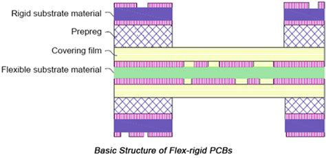
5. Rigid-Flex PCB
Rigid-flex PCBs combine the benefits of both rigid and flexible PCBs. They consist of rigid PCB sections connected by flexible PCB sections, allowing for three-dimensional assembly and improved reliability in applications that require both stability and flexibility, such as aerospace and military equipment.

PCB Manufacturing Process
The PCB manufacturing process involves several steps, each of which is critical to ensuring the quality and reliability of the final product.
1. Design and Layout
The first step in PCB manufacturing is designing the circuit and creating the PCB layout. This is typically done using electronic design automation (EDA) software, such as Altium Designer, Eagle, or KiCad. The designer must consider factors such as component placement, signal integrity, power distribution, and manufacturing constraints when creating the layout.
2. PCB Fabrication
Once the design is finalized, the PCB fabrication process begins. This involves several sub-steps:
-
Substrate Preparation: The insulating substrate, usually a sheet of fiberglass or composite epoxy, is cut to the required size and thickness. Copper Lamination: A thin layer of copper foil is laminated onto the substrate using heat and pressure.
-
Photoresist Application: A photosensitive resist material is applied to the copper-clad substrate. The photoresist hardens when exposed to light, protecting the copper beneath it from etching.
-
Exposure and Development: The PCB layout is printed onto a transparent film, called a photomask, which is placed on top of the photoresist-coated substrate. The substrate is then exposed to UV light, causing the photoresist to harden in areas not covered by the photomask. The unexposed photoresist is then removed using a chemical developer, leaving behind a pattern of hardened photoresist that matches the PCB layout.
-
Etching: The exposed copper is removed using a chemical etching process, typically with an acidic solution. The hardened photoresist protects the copper traces beneath it, resulting in a conductive pattern that matches the PCB layout.
-
Photoresist Removal: The remaining hardened photoresist is stripped away, leaving behind the copper traces on the insulating substrate.
-
Drilling: Holes are drilled through the substrate to accommodate through-hole components and vias, which connect different layers of the PCB.
-
Plating: The holes are plated with copper to create electrical connections between layers. Additional copper may be plated onto the traces to increase their thickness and current-carrying capacity.
-
Solder Mask Application: A protective solder mask is applied to the PCB, covering the copper traces while leaving the pads and other areas that require soldering exposed. This helps prevent short circuits and improves the PCB’s appearance.
-
Silkscreen: A silkscreen layer is added to the PCB, providing text and symbols that identify components, test points, and other important information.
-
Surface Finish: A surface finish, such as HASL (Hot Air Solder Leveling), ENIG (Electroless Nickel Immersion Gold), or OSP (Organic Solderability Preservative), is applied to the exposed pads to prevent oxidation and improve solderability.
3. PCB Assembly
After fabrication, the PCB is ready for assembly. This involves soldering electronic components onto the board. There are two primary methods of PCB assembly: through-hole and surface-mount.
-
Through-hole Assembly: Through-hole components have long leads that are inserted into the drilled holes on the PCB and soldered onto the opposite side. This method is well-suited for larger components and applications that require high mechanical stability.
-
Surface-mount Assembly: Surface-mount components are smaller and have short leads or no leads at all. They are soldered directly onto the pads on the surface of the PCB. Surface-mount assembly allows for higher component density and faster automated assembly processes.
4. Inspection and Testing
After assembly, the PCB undergoes rigorous inspection and testing to ensure that it meets the required specifications and functions as intended. Some common inspection and testing methods include:
- Visual inspection
- Automated optical inspection (AOI)
- X-ray inspection
- In-circuit testing (ICT)
- Functional testing
- Boundary scan testing
PCBs that pass the inspection and testing process are ready for use in the final electronic device.
Advantages of PCBs
PCBs offer several advantages over other methods of assembling electronic circuits:
-
Reliability: PCBs provide a stable and reliable platform for electronic components, reducing the risk of short circuits, loose connections, and other issues that can cause device failure.
-
Consistency: PCBs are manufactured using automated processes, ensuring consistent quality and reducing the likelihood of human error.
-
Compact Size: PCBs allow for the creation of compact, high-density electronic devices, as components can be placed close together and connected efficiently.
-
Cost-effective: PCBs are cost-effective for mass production, as the automated manufacturing process reduces labor costs and minimizes material waste.
-
Design Flexibility: PCBs can be designed to accommodate a wide range of components and circuit configurations, making them suitable for a variety of applications.
-
Improved Signal Integrity: Proper PCB Design techniques, such as careful component placement and the use of ground planes, can help reduce electromagnetic interference (EMI) and improve signal integrity.
-
Scalability: PCBs can be easily scaled up or down to meet the requirements of different applications, from small consumer devices to large industrial systems.
Applications of PCBs
PCBs are used in a vast array of electronic devices and systems, including:
- Consumer Electronics
- Smartphones
- Laptops and desktop computers
- Televisions and displays
- Gaming consoles
-
Wearable devices
-
Automotive Electronics
- Engine control units (ECUs)
- Infotainment systems
- Advanced driver assistance systems (ADAS)
-
Electric vehicle power management
-
Industrial Electronics
- Process control systems
- Automation and robotics
- Power electronics
-
Instrumentation and measurement
-
Medical Devices
- Diagnostic equipment
- Monitoring systems
- Implantable devices
-
Prosthetics
-
Aerospace and Defense
- Avionics systems
- Satellite communication
- Radar and sonar
-
Military-grade computers and electronics
-
Internet of Things (IoT)
- Smart home devices
- Industrial IoT sensors and actuators
- Wearable technology
-
Smart city infrastructure
-
Telecommunications
- Networking equipment
- Cellular base stations
- Fiber optic systems
- Satellite communication
The table below summarizes some of the key applications of PCBs across various industries:
| Industry | Applications |
|---|---|
| Consumer Electronics | Smartphones, laptops, televisions, gaming consoles |
| Automotive | Engine control units, infotainment systems, ADAS |
| Industrial Electronics | Process control systems, automation, robotics |
| Medical Devices | Diagnostic equipment, monitoring systems, implantable devices |
| Aerospace and Defense | Avionics systems, radar, military-grade electronics |
| Internet of Things | Smart home devices, industrial IoT sensors, wearable technology |
| Telecommunications | Networking equipment, cellular base stations, fiber optic systems |
Future of PCB Technology
As electronic devices continue to become more advanced and compact, PCB technology must also evolve to meet the changing demands of the industry. Some of the key trends shaping the future of PCB technology include:
-
Miniaturization: The ongoing trend towards smaller, more compact electronic devices will drive the development of even smaller and denser PCBs, with finer pitch components and thinner substrates.
-
High-speed Design: As data rates continue to increase, PCB designers will need to focus on high-speed design techniques to maintain signal integrity and minimize electromagnetic interference (EMI).
-
Advanced Materials: New substrate materials, such as high-frequency laminates and ceramic-based substrates, will be developed to meet the demands of high-speed, high-temperature, and high-reliability applications.
-
Embedded Components: The integration of passive components, such as resistors and capacitors, directly into the PCB substrate will help reduce board size and improve signal integrity.
-
3D Printing: Additive manufacturing techniques, such as 3D printing, may be used to create complex PCB structures and enable rapid prototyping.
-
Flexible and Stretchable Electronics: The development of flexible and stretchable PCBs will open up new possibilities for wearable devices, medical implants, and other applications that require conformable electronics.
-
Sustainable Manufacturing: As environmental concerns grow, PCB manufacturers will need to adopt more sustainable practices, such as using eco-friendly materials, reducing waste, and implementing energy-efficient processes.
Frequently Asked Questions (FAQ)
-
What is the difference between a PCB and a breadboard?
A PCB is a permanent, custom-designed board that has conductive traces printed on its surface to connect electronic components. A breadboard, on the other hand, is a temporary prototyping tool that allows you to quickly assemble and test electronic circuits without soldering. -
Can PCBs be repaired if they are damaged?
In some cases, PCBs can be repaired if they are damaged. The feasibility of repair depends on the extent and location of the damage, as well as the complexity of the PCB. Common repair techniques include jumper wires, conductive epoxy, and trace repair kits. However, in many cases, it may be more cost-effective to replace the damaged PCB entirely. -
What is the typical lifespan of a PCB?
The lifespan of a PCB depends on several factors, including the quality of the materials used, the manufacturing process, and the operating environment. In general, a well-designed and manufactured PCB can last for many years, often exceeding the lifespan of the electronic device it is used in. However, factors such as extreme temperatures, humidity, vibration, and electrical stress can reduce the lifespan of a PCB. -
How do I choose the right PCB manufacturer for my project?
When choosing a PCB manufacturer, consider factors such as their experience, capabilities, quality control processes, and customer support. Look for manufacturers that have experience with the type of PCB you require and can meet your specific design requirements. It’s also important to consider their turnaround time, pricing, and minimum order quantities to ensure they align with your project needs and budget. -
What are the environmental concerns associated with PCB manufacturing and disposal?
PCB manufacturing involves the use of hazardous chemicals, such as etchants, solvents, and heavy metals, which can pose risks to human health and the environment if not properly handled and disposed of. Additionally, the disposal of end-of-life PCBs can contribute to electronic waste (e-waste) if not recycled responsibly. To mitigate these concerns, PCB manufacturers and users should adhere to environmental regulations, implement proper waste management practices, and prioritize the use of eco-friendly materials and processes whenever possible.
Conclusion
Printed Circuit Boards (PCBs) are essential components in modern electronic devices, providing a reliable and efficient means of connecting electronic components. The development of PCB technology has revolutionized the electronics industry, enabling the creation of compact, high-performance devices across a wide range of applications, from consumer gadgets to advanced aerospace systems.
As electronic devices continue to evolve, so too will PCB technology. Trends such as miniaturization, high-speed design, advanced materials, and sustainable manufacturing will shape the future of PCBs, driving innovation and opening up new possibilities for the electronics industry.
By understanding the basics of PCBs, their manufacturing process, and their applications, engineers, designers, and enthusiasts can better appreciate the critical role these unassuming green boards play in our increasingly connected world.
Leave a Reply