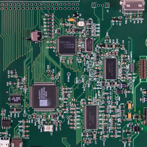
The Importance of PCBs in Modern Electronics
PCBs play a crucial role in the functioning and performance of electronic devices across industries, including:
- Consumer electronics (smartphones, laptops, televisions)
- Automotive electronics (infotainment systems, engine control units)
- Medical devices (imaging equipment, patient monitors)
- Aerospace and defense systems (avionics, radar, communications)
- Industrial automation and control (PLCs, sensors, actuators)
The use of PCBs offers several advantages over traditional point-to-point wiring:
- Compact size: PCBs allow for high-density component packaging, enabling the creation of smaller and more portable devices.
- Reliability: Properly designed and manufactured PCBs provide consistent and reliable electrical connections, reducing the risk of short circuits and component failures.
- Mass production: PCBs are well-suited for automated assembly processes, enabling the cost-effective manufacture of large quantities of identical boards.
- Signal integrity: The precise layout and routing of traces on a PCB help maintain signal integrity and minimize electromagnetic interference (EMI).
Types of PCBs
PCBs can be categorized based on various criteria, such as the number of layers, substrate material, and manufacturing process.
Number of Layers
- Single-layer PCBs: These boards have conductive traces on only one side of the substrate. They are the simplest and most affordable option, suitable for basic, low-density designs.
- Double-layer PCBs: With conductive traces on both sides of the substrate, double-layer PCBs offer increased routing flexibility and higher component density compared to single-layer boards.
- Multi-layer PCBs: These boards consist of three or more conductive layers separated by insulating layers. They are used for complex, high-speed, and high-density designs that require extensive routing and shielding.
| Layers | Advantages | Disadvantages |
|---|---|---|
| Single | Low cost, simple design | Limited routing, low component density |
| Double | Increased routing flexibility, higher component density | Higher cost than single-layer |
| Multi | Extensive routing, high-speed, high-density designs | High cost, complex design and manufacturing |
Substrate Materials
The choice of substrate material depends on the application’s requirements, such as thermal stability, dielectric constant, and mechanical strength. Common substrate materials include:
- FR-4: A composite material made of woven fiberglass and epoxy resin, FR-4 is the most widely used substrate for general-purpose PCBs.
- High-Tg FR-4: This variant of FR-4 offers improved thermal stability and is suitable for lead-free soldering processes.
- Polyimide: With excellent thermal stability and mechanical strength, polyimide is used in high-temperature and flexible PCB Applications.
- Aluminum: Aluminum PCBs provide superior heat dissipation and are used in high-power applications, such as LED lighting and motor drives.
Manufacturing Processes
- Subtractive process: The traditional PCB manufacturing method involves etching away unwanted copper from a fully copper-clad substrate, leaving behind the desired conductive traces.
- Additive process: In this method, conductive traces are selectively added onto the substrate using techniques such as inkjet printing or 3D printing. This process enables the creation of finer traces and reduces material waste.
- Semi-additive process: A combination of subtractive and additive methods, the semi-additive process involves etching a thin layer of copper and then selectively plating additional copper to form the final traces.
Designing a PCB
The PCB design process involves several key steps:
- Schematic capture: Create a schematic diagram that represents the electrical connections between components.
- Component placement: Arrange the components on the board to optimize signal routing, thermal management, and mechanical stability.
- Routing: Define the conductive traces that connect the components according to the schematic, considering factors such as trace width, spacing, and layer assignment.
- Design rule check (DRC): Verify that the PCB layout adheres to the specified design rules, such as minimum trace width and spacing, to ensure manufacturability.
- Output generation: Generate the output files required for PCB fabrication, including Gerber files, drill files, and assembly drawings.
PCB Design Software
Several software tools are available for PCB design, ranging from entry-level to professional-grade solutions:
- KiCad (open-source, free)
- Eagle (affordable, popular among hobbyists and small businesses)
- Altium Designer (professional-grade, feature-rich)
- Cadence OrCAD (professional-grade, widely used in the industry)
- Mentor Graphics PADS (professional-grade, integrated with mechanical CAD tools)

PCB Assembly
After the PCB is fabricated, the electronic components must be assembled onto the board. The assembly process typically involves the following steps:
- Solder paste application: Apply solder paste to the pads on the PCB using a stencil or screen printing process.
- Component placement: Place the components onto the PCB, either manually or using automated pick-and-place machines.
- Reflow soldering: Pass the assembled PCB through a reflow oven, which melts the solder paste and creates a permanent electrical and mechanical connection between the components and the board.
- Inspection and testing: Visually inspect the assembled PCB for defects, such as bridging or tombstoning, and perform electrical tests to verify functionality.
PCB Assembly Techniques
- Through-hole technology (THT): Components with long leads are inserted through drilled holes in the PCB and soldered on the opposite side. THT is suitable for larger components and provides strong mechanical connections.
- Surface mount technology (SMT): Components are mounted directly onto the surface of the PCB, allowing for smaller component sizes and higher-density designs. SMT is the predominant assembly method in modern electronics.
- Mixed technology: A combination of THT and SMT components on the same PCB, often used when certain components are not available in SMT packages or require additional mechanical strength.
PCB Testing and Quality Control
To ensure the reliability and functionality of assembled PCBs, various testing and quality control methods are employed:
- Automated optical inspection (AOI): Uses computer vision to detect assembly defects, such as missing components or incorrect component placement.
- X-ray inspection: Allows for the examination of solder joints and internal structures that are not visible from the surface.
- In-circuit testing (ICT): Verifies the presence, orientation, and value of individual components using a bed-of-nails fixture that makes contact with test points on the PCB.
- Functional testing: Evaluates the overall functionality of the assembled PCB by applying input signals and measuring output responses.
- Boundary scan testing: Uses built-in test circuitry (JTAG) to test the interconnections between components without the need for physical access to the PCB.
Future Trends in PCB Technology
As electronic devices continue to evolve, PCB technology must adapt to meet new challenges and demands:
- High-speed design: With the increasing prevalence of high-speed interfaces, such as USB 3.x, PCIe, and HDMI, PCB designers must pay close attention to signal integrity, impedance control, and EMI mitigation.
- Advanced packaging: Techniques such as 3D packaging, system-in-package (SiP), and package-on-package (PoP) allow for greater integration and miniaturization of electronic systems.
- Flexible and stretchable PCBs: The growing demand for wearable and implantable devices has driven the development of flexible and stretchable PCBs that can conform to non-planar surfaces and withstand repeated bending and stretching.
- Embedded components: Integrating passive components, such as resistors and capacitors, directly into the PCB substrate can save space and improve signal integrity.
- Eco-friendly materials: As environmental concerns grow, there is a push towards the use of halogen-free and lead-free materials in PCB manufacturing.
Frequently Asked Questions (FAQ)
- What is the difference between a PCB and a PCBA?
-
A PCB is the bare board without any components assembled onto it, while a PCBA (printed Circuit Board assembly) is a PCB with electronic components soldered onto it.
-
Can a PCB be repaired if damaged?
-
In some cases, minor damage to a PCB, such as a broken trace or lifted pad, can be repaired using techniques like wire jumpers or conductive epoxy. However, extensive damage may require the replacement of the entire board.
-
How long does it typically take to design and manufacture a PCB?
-
The time required for PCB design and manufacturing varies depending on the complexity of the board and the chosen fabrication process. Simple designs can be completed in a few days, while complex, multi-layer boards may take several weeks.
-
What are the most common causes of PCB failure?
-
Common causes of PCB failure include environmental factors (e.g., humidity, temperature, vibration), manufacturing defects (e.g., poor soldering, incorrect component placement), and design issues (e.g., inadequate trace spacing, improper grounding).
-
How can I ensure the reliability and longevity of my PCB design?
- To ensure PCB reliability and longevity, follow best practices in design (e.g., proper component selection, adequate trace sizing, and spacing), manufacturing (e.g., using reputable fabrication and assembly services), and testing (e.g., thorough inspection and functional testing). Additionally, consider the expected operating environment and incorporate appropriate protection measures, such as conformal coating or potting, when necessary.
Conclusion
PCBs are the backbone of modern electronics, providing a reliable and efficient means of interconnecting electronic components. Understanding the types, design, assembly, and testing of PCBs is essential for anyone involved in the development or manufacturing of electronic devices. As technology continues to advance, PCB designers and manufacturers must stay abreast of new materials, processes, and techniques to meet the ever-growing demands for smaller, faster, and more reliable electronic systems.
Leave a Reply