Introduction to Circuit Boards
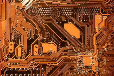
A Printed Circuit Board (PCB) is a flat board made of insulating material with conductive copper traces printed on it. These boards are used to mechanically support and electrically connect electronic components using conductive pathways, tracks or signal traces etched from copper sheets laminated onto a non-conductive substrate.
PCBs are the foundation of modern electronics and are used in nearly all electronic devices we use today, from smartphones and computers to televisions and gaming consoles. They provide a compact and efficient way to connect electronic components together.
Types of Circuit Boards
There are several types of PCBs, each with their own unique characteristics and uses:
| Type | Description |
|---|---|
| Single-sided PCB | Has conductive copper traces printed on one side of the board |
| Double-sided PCB | Has conductive copper traces printed on both sides of the board |
| Multi-layer PCB | Has multiple layers of conductive copper traces separated by insulating layers |
| Flexible PCB | Made from flexible materials like polyimide, allowing the board to bend and flex |
| Rigid-Flex PCB | Combines rigid and flexible sections for unique applications |
How are PCBs made?
The process of creating a PCB involves several steps:
-
Design: The circuit is designed using specialized software called Electronic Design Automation (EDA) tools. The design includes the placement of components and the routing of copper traces.
-
Printing: The design is printed onto a transparent film called a photomask.
-
Etching: The copper-clad board is coated with a light-sensitive material called photoresist. The photomask is placed on top of the board and exposed to UV light, hardening the photoresist where the copper traces should remain. The unhardened photoresist is then washed away, exposing the unwanted copper.
-
Plating: The board is placed in an electrolytic bath, which deposits a thin layer of copper onto the exposed traces, making them thicker and more durable.
-
Drilling: Holes are drilled into the board to allow components to be mounted and connected to the copper traces.
-
Soldering: Components are placed onto the board and soldered to the copper traces, creating a complete circuit.
PCB Manufacturing Process
| Step | Description |
|---|---|
| Design | Circuit design using EDA tools |
| Printing | Design printed onto photomask |
| Etching | Unwanted copper removed using photoresist and UV light |
| Plating | Copper traces thickened through electroplating |
| Drilling | Holes drilled for component mounting |
| Soldering | Components soldered to the board |
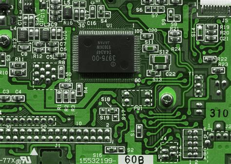
Components of a PCB
A typical PCB consists of several key components:
Substrate
The substrate is the insulating material that forms the base of the PCB. It is typically made from materials like FR-4 (a type of fiberglass), which provides a stable and durable foundation for the copper traces and components.
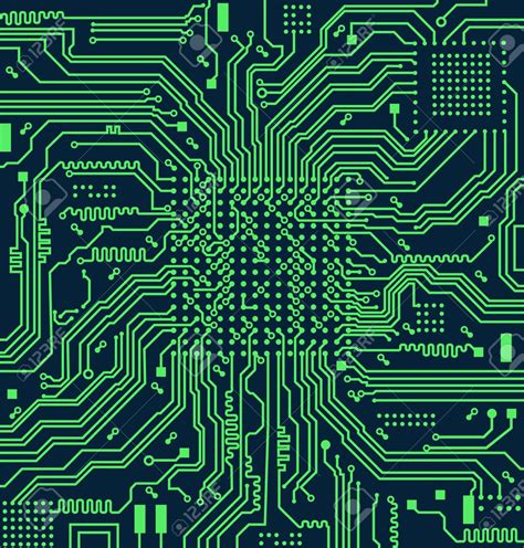
Copper Traces
Copper traces are the conductive pathways that connect the various components on the PCB. They are typically made from a thin layer of copper foil that is laminated onto the substrate and then etched into the desired pattern.
Solder Mask
The solder mask is a protective layer that covers the copper traces, leaving only the areas where components will be soldered exposed. This layer helps to prevent short circuits and makes it easier to solder components to the board.
Silkscreen
The silkscreen is a layer of text and symbols printed onto the PCB that provides information about the board, such as component labels, logos, and other identifying marks.
Vias
Vias are small holes drilled through the PCB that allow copper traces on different layers to connect. They are often plated with copper to ensure a reliable electrical connection.
Components
The components are the various electronic parts that are mounted onto the PCB, such as resistors, capacitors, integrated circuits, and connectors. These components are soldered to the copper traces to create a complete circuit.

Advantages of Using PCBs
PCBs offer several advantages over other methods of connecting electronic components:
-
Compact Size: PCBs allow for a high density of components to be mounted in a small space, making them ideal for use in portable electronic devices.
-
Reliability: The copper traces on a PCB are more reliable than individual wires, as they are less likely to break or become disconnected.
-
Consistency: PCBs are manufactured using automated processes, ensuring a high level of consistency between boards.
-
Cost-effective: Once the initial design costs are paid, PCBs can be mass-produced at a relatively low cost per unit.
-
Ease of Repair: If a component fails, it can be easily replaced without having to rewire the entire circuit.
Applications of PCBs
PCBs are used in a wide range of electronic devices and systems, including:
- Computers and laptops
- Smartphones and tablets
- Televisions and home entertainment systems
- Gaming consoles and controllers
- Medical devices and equipment
- Automotive electronics
- Industrial control systems
- Aerospace and military applications
As technology continues to advance, the demand for smaller, more complex, and more reliable electronic devices will continue to drive the development of new PCB technologies and manufacturing processes.
Frequently Asked Questions (FAQ)
-
What is the difference between a single-sided and double-sided PCB?
A single-sided PCB has copper traces on only one side of the substrate, while a double-sided PCB has copper traces on both sides. Double-sided PCBs allow for more complex circuits and higher component density. -
What is the purpose of the solder mask on a PCB?
The solder mask is a protective layer that covers the copper traces, leaving only the areas where components will be soldered exposed. It helps to prevent short circuits and makes it easier to solder components to the board. -
Can PCBs be recycled?
Yes, PCBs can be recycled. The process involves separating the various materials, such as copper, gold, and plastic, which can then be reused in new products. However, due to the complex nature of PCBs, recycling them can be challenging and costly. -
How long does it take to manufacture a PCB?
The time required to manufacture a PCB depends on several factors, such as the complexity of the design, the number of layers, and the manufacturing process used. Simple, single-sided PCBs can be produced in a matter of days, while complex, multi-layer boards may take several weeks. -
What is the future of PCB technology?
As electronic devices continue to become smaller, more powerful, and more complex, the demand for advanced PCB technologies will continue to grow. Some of the emerging trends in PCB technology include the use of embedded components, high-density interconnects (HDI), and flexible and stretchable circuits for wearable electronics.
Conclusion
Printed Circuit Boards (PCBs) are an essential component of modern electronics, providing a compact, reliable, and cost-effective way to connect electronic components. By understanding the basics of how PCBs are designed, manufactured, and used, children can gain a better appreciation for the technology that powers the devices they use every day. As PCB technology continues to evolve, it will play an increasingly important role in shaping the future of electronics and the world around us.
Leave a Reply