Introduction to PCB and Its Meaning
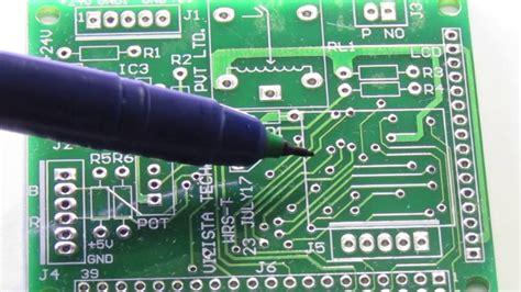
PCB stands for Printed Circuit Board. It is a fundamental component in virtually all modern electronic devices, serving as the foundation upon which electronic components are mounted and interconnected. PCBs provide mechanical support and electrical connectivity for electronic components, enabling the creation of complex electronic circuits in a compact and organized manner.
Key Points about PCBs
- PCBs are essential in modern electronics
- They provide mechanical support and electrical connectivity
- PCBs enable the creation of complex circuits in a compact form factor
The History and Evolution of PCBs
Early Developments in Circuit Board Technology
The concept of printed circuit boards can be traced back to the early 20th century. In 1903, German inventor Albert Hanson filed a patent for a method of creating electrical connections on an insulating board using conductive metal strips. This early concept laid the foundation for the development of modern PCBs.
The Introduction of Printed Circuit Boards
In the 1940s, during World War II, the demand for compact and reliable electronic equipment for military applications drove the development of printed circuit boards. Paul Eisler, an Austrian engineer, is credited with inventing the first printed circuit board in 1943. Eisler’s design involved printing conductive ink onto a non-conductive substrate, creating a pattern of electrical connections.
The Transition to Modern PCBs
Throughout the 1950s and 1960s, PCB manufacturing techniques evolved rapidly. The introduction of photoresist and etching processes allowed for more precise and intricate circuit patterns. The use of copper-clad laminates, such as FR-4, became common, providing a stable and durable substrate for PCBs.
| Era | Key Developments |
|---|---|
| Early 20th century | Concept of electrical connections on insulating boards |
| 1940s | Invention of printed circuit boards by Paul Eisler |
| 1950s-1960s | Introduction of photoresist, etching, and copper-clad laminates |
The Structure and Components of a PCB
The PCB Substrate
The substrate is the foundation of a PCB, providing mechanical support and electrical insulation. Common substrate materials include:
- FR-4: A composite material made of woven fiberglass and epoxy resin, known for its durability and thermal stability.
- Polyimide: A flexible polymer used for flexible PCBs.
- Ceramic: Used in high-frequency and high-temperature applications.
Copper Layers and Traces
PCBs consist of one or more layers of copper, which are laminated onto the substrate. These copper layers are etched to form the desired circuit pattern, creating conductive traces that connect the electronic components. The number of copper layers determines the complexity and density of the PCB.
| Number of Layers | PCB Type |
|---|---|
| 1-2 | Single-sided or double-sided PCBs |
| 4-8 | Multi-layer PCBs |
| 10+ | High-density interconnect (HDI) PCBs |
Solder Mask and Silkscreen
- Solder Mask: A protective coating applied over the copper traces, leaving only the exposed pads for component soldering. It prevents short circuits and provides insulation.
- Silkscreen: A printed layer on top of the solder mask that includes text, symbols, and component outlines for easy identification and assembly.

PCB design and Manufacturing Process
Schematic Design and Capture
The PCB design process begins with creating a schematic diagram, which represents the electrical connections and components of the circuit. Engineers use electronic design automation (EDA) software to capture the schematic and define the interconnections between components.
PCB Layout and Routing
Once the schematic is complete, the PCB layout process begins. PCB designers use specialized software to place components and route the copper traces on the PCB. The layout must consider factors such as signal integrity, power distribution, and manufacturability.
PCB Fabrication Steps
- PCB fabrication involves several key steps:
- Printing the circuit pattern onto the copper-clad laminate using photoresist.
- Etching away the unwanted copper, leaving only the desired traces.
- Drilling holes for through-hole components and vias.
- Applying solder mask and silkscreen layers.
- Surface finishing, such as HASL (Hot Air Solder Leveling) or ENIG (Electroless Nickel Immersion Gold), to protect the exposed copper and facilitate soldering.
PCB Assembly and Soldering
After fabrication, the PCB is ready for component assembly. Surface mount components are placed onto the PCB using pick-and-place machines, while through-hole components are inserted manually. The assembled PCB then undergoes soldering, typically using reflow ovens for surface mount components and wave soldering for through-hole components.
Types of PCBs and Their Applications
Single-Sided PCBs
Single-sided PCBs have conductive traces on only one side of the substrate. They are the simplest and most cost-effective type of PCB, suitable for basic electronic circuits and low-density designs.
Double-Sided PCBs
Double-sided PCBs have conductive traces on both sides of the substrate, allowing for higher component density and more complex circuits. The two sides are connected using through-hole vias.
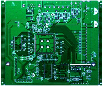
Multi-Layer PCBs
Multi-layer PCBs consist of multiple layers of conductive traces sandwiched between insulating layers. They offer high component density and are used in complex electronic devices, such as smartphones, computers, and automotive electronics.
| PCB Type | Number of Layers | Applications |
|---|---|---|
| Single-Sided | 1 | Basic electronic circuits, low-density designs |
| Double-Sided | 2 | Higher component density, more complex circuits |
| Multi-Layer | 4+ | Complex electronic devices, high-density designs |
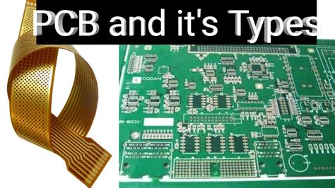
Flexible PCBs
Flexible PCBs, also known as flex circuits, are made using flexible substrate materials like polyimide. They can bend and conform to various shapes, making them ideal for applications where flexibility and space constraints are critical, such as wearable electronics and medical devices.
Rigid-Flex PCBs
Rigid-flex PCBs combine the benefits of both rigid and flexible PCBs. They consist of rigid PCB sections connected by flexible PCB sections, allowing for three-dimensional packaging and improved reliability in applications with limited space or mechanical stress.
PCB Design Considerations and Best Practices
Signal Integrity and Impedance Control
Signal integrity is crucial in PCB design, especially for high-speed and high-frequency circuits. Designers must consider factors such as trace width, spacing, and impedance matching to minimize signal reflections, crosstalk, and electromagnetic interference (EMI).
Power Distribution and Decoupling
Proper power distribution is essential to ensure stable and clean power delivery to all components on the PCB. Designers use power planes, ground planes, and decoupling capacitors to minimize voltage fluctuations and reduce noise.
Thermal Management
Thermal management is critical in PCB design to prevent overheating and ensure reliable operation. Techniques such as using thermal vias, copper pours, and heat sinks help dissipate heat generated by components.
Design for Manufacturing (DFM)
Design for Manufacturing (DFM) principles optimize the PCB design for efficient and cost-effective manufacturing. This includes considering factors such as component placement, trace spacing, and soldermask design to minimize manufacturing defects and improve yield.
The Future of PCB Technology
Advanced Materials and Substrates
As electronic devices become more complex and demanding, new materials and substrates are being developed to improve PCB performance. Examples include high-frequency laminates, thermally conductive substrates, and embedded component technologies.
3D Printing and Additive Manufacturing
3D printing and additive manufacturing techniques are being explored for PCB fabrication. These methods have the potential to enable rapid prototyping, custom designs, and the integration of unique geometries and materials.
Miniaturization and High-Density Interconnects (HDI)
The trend towards miniaturization continues to drive the development of high-density interconnect (HDI) PCBs. HDI PCBs feature finer trace widths, smaller via sizes, and higher component densities, enabling the creation of compact and highly integrated electronic devices.
FAQ
1. What is the difference between a PCB and a circuit board?
A PCB (Printed Circuit Board) is a specific type of circuit board that uses conductive traces printed or etched onto a non-conductive substrate to create electrical connections. The term “circuit board” is a more general term that encompasses various types of boards used to create electrical circuits, including PCBs, breadboards, and stripboards.
2. Are all PCBs green in color?
No, not all PCBs are green. The green color commonly associated with PCBs comes from the solder mask, which is a protective coating applied over the copper traces. While green is a popular color choice for solder mask, PCBs can come in various colors, such as red, blue, black, or white, depending on the manufacturer and the specific application requirements.
3. Can PCBs be recycled?
Yes, PCBs can be recycled. However, due to the complex mixture of materials used in PCBs, including metals, plastics, and hazardous substances, recycling PCBs requires specialized processes and facilities. Proper recycling of PCBs is essential to recover valuable materials, such as copper and precious metals, and to prevent environmental contamination from improper disposal.
4. What is the typical lifespan of a PCB?
The lifespan of a PCB depends on various factors, such as the quality of materials used, the manufacturing process, the operating environment, and the specific application. Generally, a well-designed and manufactured PCB can last for several years to decades, depending on the intended use. However, factors like exposure to harsh environments, mechanical stress, and power surges can reduce the lifespan of a PCB.
5. How do I choose the right PCB manufacturer?
When choosing a PCB manufacturer, consider the following factors:
- Technical capabilities: Ensure the manufacturer can accommodate your specific PCB requirements, such as the number of layers, materials, and surface finishes.
- Quality control: Look for manufacturers with robust quality control processes and certifications, such as ISO 9001 and IPC standards.
- Lead time and pricing: Compare lead times and pricing among manufacturers to find the best balance between cost and delivery speed.
- Customer support: Choose a manufacturer with responsive and knowledgeable customer support to assist you throughout the PCB design and manufacturing process.
- Reputation and reviews: Research the manufacturer’s reputation and read reviews from previous customers to gauge their reliability and quality of service.
Conclusion
PCBs have revolutionized the electronics industry, enabling the creation of compact, reliable, and complex electronic devices. From their early beginnings in the 20th century to the advanced manufacturing techniques and materials used today, PCBs continue to evolve to meet the ever-growing demands of modern electronics.
Understanding the structure, components, and manufacturing process of PCBs is essential for engineers, designers, and anyone involved in the development of electronic products. By considering factors such as signal integrity, power distribution, thermal management, and design for manufacturing, PCB designers can create high-quality and reliable circuits that form the backbone of our digital world.
As technology advances, the future of PCBs looks promising, with innovations in materials, manufacturing techniques, and miniaturization driving the development of even more sophisticated and compact electronic devices. By staying informed about the latest trends and best practices in PCB design and manufacturing, engineers and designers can create cutting-edge products that shape the future of electronics.
Leave a Reply