The Basics of PCB design
PCB Layers and Materials
A PCB typically consists of multiple layers of conductive and insulating materials. The most common materials used in PCB manufacturing are:
- Copper (conductive layer)
- FR-4 (insulating substrate)
- Solder mask (protective coating)
- Silkscreen (text and symbols)
The number of layers in a PCB can vary depending on the complexity of the circuit. Single-layer and double-layer PCBs are suitable for simple designs, while multi-layer PCBs (4, 6, 8, or more layers) are used for more complex circuits.
PCB Design Software
To create a PCB design, engineers use specialized software tools called Electronic Design Automation (EDA) software. Some popular EDA software packages include:
- Altium Designer
- KiCad
- Eagle
- OrCAD
These software tools allow designers to create schematic diagrams, define component footprints, route traces, and generate manufacturing files.
PCB Design Process
Schematic Design
The first step in PCB design is creating a schematic diagram. A schematic represents the logical connections between electronic components using standardized symbols. It helps to visualize the circuit’s functionality and serves as a blueprint for the PCB layout.
Component Selection and Footprint Creation
Once the schematic is complete, the next step is to select appropriate components and create their footprints. A footprint is the physical representation of a component on the PCB, including its pad size, shape, and spacing. Footprints must be accurate to ensure proper component placement and solderability.
PCB Layout
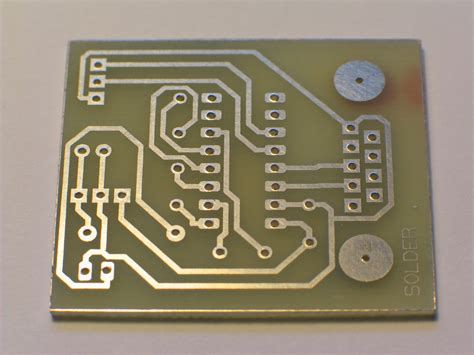
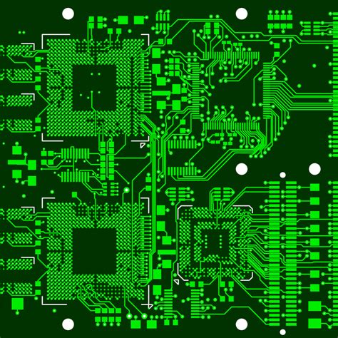
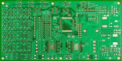
With the schematic and component footprints ready, the designer can start the PCB layout process. This involves placing components on the board and routing traces to connect them according to the schematic. The layout must follow various design rules to ensure manufacturability, reliability, and performance. Some key considerations during PCB layout include:
- Component placement and orientation
- Trace width and spacing
- Via size and placement
- Power and ground plane design
- Signal integrity and electromagnetic compatibility (EMC)
Design Rule Check (DRC) and Gerber File Generation
After completing the PCB layout, the designer must run a Design Rule Check (DRC) to verify that the design meets all the specified manufacturing constraints. DRC helps to identify and correct any potential issues before sending the design for fabrication.
Finally, the designer generates Gerber files, which are the industry-standard format for PCB manufacturing. Gerber files contain all the necessary information for the PCB fabrication process, including copper layers, solder mask, silkscreen, and drill data.

Advanced PCB Design Techniques
High-Speed PCB Design
As electronic devices operate at increasingly higher frequencies, high-speed PCB design techniques become essential. High-speed signals are more susceptible to signal integrity issues, such as crosstalk, reflections, and electromagnetic interference (EMI). To mitigate these issues, designers must consider:
- Controlled impedance traces
- Differential pair routing
- Proper termination and matching
- Ground plane design and isolation
Thermal Management
Thermal management is crucial for PCBs that dissipate significant amounts of heat, such as power electronics or high-performance digital circuits. Proper thermal management ensures reliable operation and prevents component failure due to overheating. Some techniques for thermal management include:
- Using thermal vias to transfer heat from components to the PCB’s copper layers
- Incorporating heat sinks and cooling fans
- Selecting components with appropriate power ratings and temperature specifications
Flex and Rigid-Flex PCBs
Flex and rigid-flex PCBs are specialized designs that offer increased flexibility and durability compared to traditional rigid PCBs. Flex PCBs use thin, flexible substrates that can bend and conform to various shapes, making them ideal for applications with limited space or movable parts. Rigid-flex PCBs combine both rigid and flexible sections, allowing for complex 3D structures and improved reliability in demanding environments.

PCB Manufacturing and Assembly
PCB Fabrication
Once the PCB design is complete and Gerber files are generated, the next step is PCB fabrication. The fabrication process involves several stages:
- Substrate preparation: The base material (usually FR-4) is cut to the desired size and shape.
- Copper deposition: Copper foil is laminated onto the substrate using heat and pressure.
- Photoresist application: A light-sensitive polymer (photoresist) is applied to the copper surface.
- Exposure and development: The photoresist is exposed to UV light through a photomask, which hardens the exposed areas. The unexposed areas are then removed using a developer solution.
- Etching: The exposed copper is etched away using a chemical solution, leaving only the desired traces and pads.
- Solder mask application: A protective solder mask is applied to the PCB surface, leaving only the exposed pads for component soldering.
- Silkscreen printing: Text and symbols are printed onto the PCB surface using silkscreen ink.
- Surface finish: A surface finish (e.g., HASL, ENIG, or OSP) is applied to the exposed pads to improve solderability and protect against oxidation.
PCB Assembly
After fabrication, the PCB is ready for assembly. The assembly process involves placing components onto the board and soldering them in place. There are two main methods for PCB assembly:
- Through-hole assembly: Components with long leads are inserted through holes in the PCB and soldered on the opposite side.
- Surface-mount assembly: Components with small, flat leads (SMD components) are placed directly onto pads on the PCB surface and soldered using a reflow oven or wave soldering machine.
Automated assembly processes, such as pick-and-place machines and reflow soldering, are commonly used for high-volume production. Manual assembly techniques, like hand soldering, are suitable for low-volume or prototype builds.

Frequently Asked Questions (FAQ)
1. What is the difference between a schematic and a PCB layout?
A schematic is a logical representation of a circuit, showing the connections between components using standardized symbols. A PCB layout, on the other hand, is the physical representation of the circuit on a printed Circuit Board, including component placement, trace routing, and copper layers.
2. What are the benefits of using a multi-layer PCB?
Multi-layer PCBs offer several advantages over single or double-layer boards:
– Increased circuit density and complexity
– Improved signal integrity and reduced crosstalk
– Better power and ground distribution
– Enhanced thermal management
– Reduced board size and weight
3. What is controlled impedance in PCB design?
Controlled impedance refers to the precise management of the characteristic impedance of PCB traces. It is essential for high-speed signals to maintain signal integrity and minimize reflections. Controlled impedance is achieved by carefully designing the trace width, spacing, and dielectric thickness of the PCB.
4. What is the purpose of a solder mask on a PCB?
A solder mask is a protective coating applied to the PCB surface, leaving only the exposed pads for component soldering. It serves several purposes:
– Prevents solder bridges and short circuits
– Protects the copper traces from oxidation and environmental damage
– Provides electrical insulation between adjacent traces
– Improves the aesthetics of the PCB
5. What are the common surface finishes used in PCB manufacturing?
The most common surface finishes used in PCB manufacturing are:
– HASL (Hot Air Solder Leveling): A tin-lead alloy is applied to the exposed pads using a hot air process.
– ENIG (Electroless Nickel Immersion Gold): A layer of nickel is plated onto the copper, followed by a thin layer of gold.
– OSP (Organic Solderability Preservative): A thin, organic coating is applied to the exposed copper to prevent oxidation.
– Immersion Silver: A thin layer of silver is chemically deposited onto the copper surface.
– Immersion Tin: A thin layer of tin is chemically deposited onto the copper surface.
| Surface Finish | Advantages | Disadvantages |
|---|---|---|
| HASL | – Low cost – Good solderability – Robust |
– Uneven surface – Not suitable for fine-pitch components |
| ENIG | – Flat surface – Excellent solderability – Long shelf life |
– Higher cost – Possible nickel corrosion (black pad) |
| OSP | – Low cost – Flat surface – Suitable for fine-pitch components |
– Limited shelf life – Possible solderability issues |
| Immersion Silver | – Flat surface – Good solderability – Suitable for fine-pitch components |
– Higher cost – Possible silver migration |
| Immersion Tin | – Flat surface – Good solderability – Suitable for fine-pitch components |
– Limited shelf life – Possible tin whiskers |
In conclusion, the working principle of PCB design involves a systematic approach to creating a functional and reliable Printed Circuit Board. By understanding the basics of PCB materials, design software, and the design process itself, engineers can create high-quality PCBs that meet the requirements of modern electronic devices. Advanced techniques, such as high-speed design, thermal management, and flex PCBs, further expand the possibilities of PCB design. Finally, the PCB manufacturing and assembly processes bring the design to life, resulting in a finished product ready for use in various applications.

Leave a Reply