Understanding Printed Circuit Boards (PCBs)
Printed Circuit Boards, commonly referred to as PCBs, are the backbone of modern electronic devices. They are essential components in nearly all electronic equipment, from smartphones and computers to medical devices and aerospace systems. In this comprehensive article, we will delve into the world of PCBs, exploring their definition, history, manufacturing process, applications, and future trends.
What is a Printed Circuit Board (PCB)?
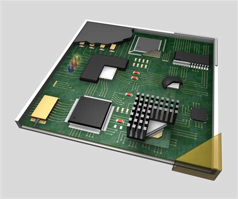
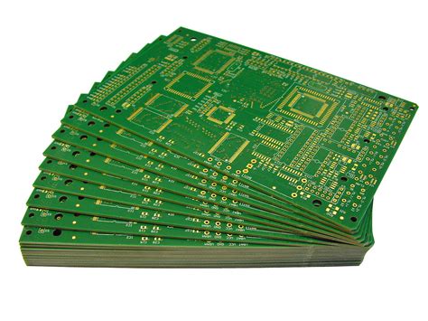
A Printed Circuit Board is a flat, thin board made of insulating material, such as fiberglass or composite epoxy, with conductive pathways etched or printed onto its surface. These conductive pathways, called traces, connect various electronic components, such as resistors, capacitors, and integrated circuits (ICs), to form a complete electronic circuit.
PCBs serve as the foundation for mounting and interconnecting electronic components, providing both mechanical support and electrical connections. They eliminate the need for complex wiring and soldering, making electronic devices more compact, reliable, and efficient.
History of PCBs
The concept of printed circuits dates back to the early 20th century. In 1903, German inventor Albert Hanson filed a patent for a method of creating conductive patterns on an insulating substrate. However, it wasn’t until the 1940s that PCBs began to gain widespread adoption.
During World War II, the United States military heavily invested in the development of PCB technology to improve the reliability and efficiency of electronic equipment used in warfare. In 1943, Austrian engineer Paul Eisler developed the first modern PCB while working on a radio set for the British military.
After the war, PCB technology continued to evolve, with the introduction of double-sided boards, plated-through holes, and multi-layer boards. The rise of the consumer electronics industry in the 1960s and 1970s further drove the growth and advancement of PCB manufacturing techniques.
PCB Manufacturing Process
The manufacturing process of PCBs involves several key steps, each requiring precision and attention to detail. The primary stages of PCB fabrication include:
-
Design and Layout: The PCB design is created using specialized software, such as Altium Designer or Eagle CAD. The layout includes the placement of components, routing of traces, and the creation of solder masks and silkscreen layers.
-
Substrate Preparation: The substrate material, typically a laminate of fiberglass and epoxy resin, is cut to the desired size and shape. Copper foil is then laminated onto one or both sides of the substrate using heat and pressure.
-
Photoresist Application: A light-sensitive photoresist is applied to the copper-clad board. The photoresist is then exposed to UV light through a photomask, which contains the desired circuit pattern.
-
Etching: The exposed copper is etched away using a chemical solution, leaving only the desired conductive traces on the board.
-
Drilling: Holes are drilled through the board to accommodate through-hole components and provide interconnections between layers in multi-layer boards.
-
Plating: The drilled holes are plated with copper to create conductive pathways between layers. Additional plating, such as tin-lead or gold, may be applied to improve solderability and protect the copper traces.
-
Solder Mask and Silkscreen: A solder mask, typically green in color, is applied to the board to protect the copper traces and prevent solder bridges. A silkscreen layer is then added to provide component labels and other identifying marks.
-
Surface Finishing: The exposed copper areas, such as pads and contacts, are coated with a protective finish, such as hot air solder leveling (HASL), immersion silver, or electroless nickel immersion gold (ENIG), to prevent oxidation and enhance solderability.
-
Electrical Testing: The completed PCB undergoes electrical testing to ensure proper functionality and adherence to design specifications.
Types of PCBs
PCBs can be classified based on several factors, including the number of layers, materials used, and manufacturing techniques employed. Some common types of PCBs include:
-
Single-sided PCBs: These boards have conductive traces on only one side of the substrate. They are the simplest and most cost-effective type of PCB, suitable for basic electronic projects and low-density designs.
-
Double-sided PCBs: These boards have conductive traces on both sides of the substrate, allowing for higher component density and more complex circuits. The two sides are interconnected using plated-through holes.
-
Multi-layer PCBs: These boards consist of three or more layers of conductive traces, separated by insulating layers. They offer the highest component density and are used in complex, high-performance electronic devices. Multi-layer PCBs can have up to 50 layers or more, depending on the application.
-
Flexible PCBs: These boards are made using flexible substrate materials, such as polyimide or polyester, allowing them to bend and conform to various shapes. Flexible PCBs are commonly used in wearable electronics, medical devices, and aerospace applications.
-
Rigid-Flex PCBs: These boards combine the benefits of both rigid and flexible PCBs. They consist of rigid sections connected by flexible sections, enabling 3D packaging and improved reliability in applications that require movement or vibration.
PCB Materials
The choice of materials used in PCB fabrication depends on the specific requirements of the application, such as operating temperature, frequency, and environmental conditions. Some common PCB materials include:
-
FR-4: A composite material made of woven fiberglass and epoxy resin, FR-4 is the most widely used substrate material for PCBs. It offers good mechanical strength, electrical insulation, and thermal stability.
-
High-Tg FR-4: This variant of FR-4 has a higher glass transition temperature (Tg), making it suitable for applications that require higher operating temperatures or improved thermal reliability.
-
Polyimide: A high-performance polymer, polyimide is used in flexible PCBs and applications that demand excellent thermal and chemical resistance.
-
PTFE (Teflon): PCBs made with PTFE substrates offer superior high-frequency performance and low dielectric loss, making them ideal for RF and microwave applications.
-
Aluminum: Metal-core PCBs (MCPCBs) use aluminum substrates to improve heat dissipation in high-power applications, such as LED lighting and power electronics.
PCB Applications
PCBs are used in a wide range of industries and applications, from consumer electronics to industrial automation and aerospace systems. Some notable applications include:
-
Consumer Electronics: PCBs are found in smartphones, tablets, laptops, televisions, gaming consoles, and home appliances.
-
Automotive: Modern vehicles rely heavily on PCBs for engine control, infotainment systems, sensors, and advanced driver assistance systems (ADAS).
-
Medical Devices: PCBs are essential components in medical equipment, such as patient monitors, imaging systems, and implantable devices.
-
Industrial Automation: PCBs are used in programmable logic controllers (PLCs), human-machine interfaces (HMIs), sensors, and actuators in industrial control systems.
-
Aerospace and Defense: High-reliability PCBs are employed in satellites, aircraft, missiles, and military communication systems.
-
Internet of Things (IoT): PCBs are the foundation for IoT devices, enabling the connection and communication of everyday objects over the internet.
Future Trends in PCB Technology
As electronic devices continue to evolve, so do the technologies and techniques used in PCB manufacturing. Some notable trends shaping the future of PCBs include:
-
Miniaturization: The demand for smaller, more compact electronic devices is driving the development of advanced packaging techniques, such as system-in-package (SiP) and 3D packaging, which integrate multiple components and functionalities onto a single PCB.
-
High-Density Interconnect (HDI): HDI PCBs feature finer traces, smaller vias, and higher component density, enabling the creation of more complex and compact electronic systems.
-
Embedded Components: Passive components, such as resistors and capacitors, can be embedded within the PCB substrate, further reducing the size and improving the performance of electronic devices.
-
Additive Manufacturing: 3D printing technologies, such as inkjet and aerosol jet printing, are being explored as alternative methods for PCB fabrication, offering faster prototyping and greater design flexibility.
-
Advanced Materials: The development of new substrate materials, such as high-frequency laminates and thermally conductive materials, is enabling the creation of PCBs for specialized applications, such as 5G communications and high-power electronics.
-
Environmental Sustainability: There is a growing emphasis on the use of eco-friendly materials and processes in PCB manufacturing, such as halogen-free laminates and lead-free solders, to reduce the environmental impact of electronic waste.
Frequently Asked Questions (FAQ)
-
What is the difference between a PCB and a printed wiring board (PWB)?
A PWB is a more general term that encompasses any board with conductive pathways, including wire-wrapped and point-to-point wired boards. A PCB specifically refers to a board with conductive traces printed or etched onto the substrate. -
Can PCBs be repaired?
While it is possible to repair PCBs, the feasibility and cost-effectiveness of the repair depend on the extent of the damage and the complexity of the board. In many cases, replacing the entire PCB is more practical than attempting a repair. -
What is the typical lifespan of a PCB?
The lifespan of a PCB depends on various factors, such as the quality of materials used, the manufacturing process, and the operating environment. Well-designed and manufactured PCBs can last for several decades, while those exposed to harsh conditions or subjected to frequent thermal cycling may have a shorter lifespan. -
How do I choose the right PCB manufacturer?
When selecting a PCB manufacturer, consider factors such as their experience, capabilities, quality control processes, and certifications. Look for manufacturers that specialize in the type of PCB you require and have a proven track record of delivering high-quality boards on time. -
What is the minimum feature size achievable in PCB manufacturing?
The minimum feature size, such as trace width and spacing, depends on the capabilities of the PCB manufacturer and the chosen fabrication technology. Advanced HDI PCBs can achieve trace widths and spacings as small as 50 microns (0.05 mm), while standard PCBs typically have a minimum feature size of around 100 microns (0.1 mm).
Conclusion
Printed Circuit Boards have revolutionized the electronics industry, enabling the creation of compact, reliable, and efficient electronic devices. From their humble beginnings in the early 20th century to their ubiquitous presence in modern technology, PCBs have undergone a remarkable evolution.
As we continue to push the boundaries of electronic design and functionality, PCB technology will undoubtedly play a crucial role in shaping the future of electronics. By understanding the fundamentals of PCBs, their manufacturing processes, and the latest trends in the industry, engineers and designers can create innovative solutions that meet the ever-growing demands of the digital age.
| PCB Type | Advantages | Disadvantages |
|---|---|---|
| Single-sided | – Low cost – Simple design – Easy to manufacture |
– Limited component density – Limited routing options |
| Double-sided | – Higher component density – Improved routing options – Better signal integrity |
– Higher manufacturing cost than single-sided – More complex design and layout |
| Multi-layer | – Highest component density – Excellent signal integrity – Ideal for complex circuits |
– Highest manufacturing cost – Complex design and layout – Longer lead times |
| Flexible | – Conformable to various shapes – Lightweight and thin – Resistant to vibration and shock |
– Limited component density – Higher cost than rigid PCBs – Requires specialized design and manufacturing |
| Rigid-Flex | – Combines benefits of rigid and flexible PCBs – Enables 3D packaging – Improved reliability in dynamic environments |
– Higher cost than standard rigid PCBs – Complex design and manufacturing process |
As the demand for more advanced and efficient electronic devices continues to grow, the role of PCBs in engineering will only become more critical. By staying informed about the latest developments in PCB technology and manufacturing, engineers can create innovative solutions that push the boundaries of what is possible in the world of electronics.
Leave a Reply