Introduction to PCB and Its Role in Projects
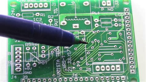
A PCB, which stands for Printed Circuit board, is a fundamental component in nearly all modern electronic devices and projects. PCBs provide a way to mechanically support and electrically connect electronic components using conductive pathways, tracks, or signal traces etched from copper sheets laminated onto a non-conductive substrate.
PCBs play a crucial role in project development by enabling the creation of complex circuits in a compact and organized manner. They serve as the backbone of electronic projects, allowing components to communicate with each other efficiently and reliably.
Key Functions of PCBs in Projects
-
Interconnectivity: PCBs provide a means to connect various electronic components, such as resistors, capacitors, integrated circuits (ICs), and sensors, allowing them to interact and function as a complete system.
-
Space optimization: By using PCBs, project designers can organize components in a compact and efficient layout, minimizing the overall size of the device while maximizing functionality.
-
Signal integrity: Well-designed PCBs ensure that electrical signals travel efficiently between components with minimal interference, distortion, or loss, resulting in better system performance and reliability.
-
Heat dissipation: PCBs can be designed with thermal considerations in mind, incorporating features such as heat sinks, thermal vias, or specialized substrates to help dissipate heat generated by components, preventing overheating and prolonging the lifespan of the device.
Types of PCBs Used in Projects
There are several types of PCBs used in various projects, each with its own unique characteristics and applications. Understanding the differences between these types can help project developers choose the most suitable PCB for their specific needs.
Single-layer PCBs
Single-layer PCBs, also known as single-sided PCBs, have conductive copper traces on only one side of the substrate. These PCBs are the simplest and most cost-effective option, making them ideal for basic projects or prototypes with low complexity.
Advantages:
– Low cost
– Easy to design and manufacture
– Suitable for simple circuits
Disadvantages:
– Limited routing options
– Not suitable for complex circuits or high-density designs
– Larger footprint compared to multi-layer PCBs
Double-layer PCBs
Double-layer PCBs, also called double-sided PCBs, have conductive copper traces on both sides of the substrate. These PCBs offer more routing options and higher component density compared to single-layer PCBs, making them suitable for more complex projects.
Advantages:
– Increased routing options and component density
– Better signal integrity
– Smaller footprint compared to single-layer PCBs
Disadvantages:
– Higher cost than single-layer PCBs
– More complex design and manufacturing process
Multi-layer PCBs
Multi-layer PCBs consist of three or more conductive layers separated by insulating layers. These PCBs offer the highest level of complexity and density, making them ideal for advanced projects with strict space constraints or high-speed signal requirements.
Advantages:
– High component density
– Excellent signal integrity
– Ideal for complex circuits and high-speed applications
– Reduced electromagnetic interference (EMI)
Disadvantages:
– High cost
– Complex design and manufacturing process
– Longer lead times
Flexible PCBs
Flexible PCBs, or flex PCBs, are made using a flexible substrate material, such as polyimide, allowing the PCB to bend and conform to various shapes. These PCBs are ideal for projects requiring non-planar or movable components, such as wearable devices or compact electronics.
Advantages:
– Conformable to various shapes
– Lightweight and thin
– Resistant to vibration and shock
– Ideal for wearable devices and compact electronics
Disadvantages:
– Higher cost compared to rigid PCBs
– Limited component options
– More complex design and manufacturing process
Rigid-Flex PCBs
Rigid-flex PCBs combine the benefits of both rigid and flexible PCBs by incorporating rigid and flexible layers in a single board. This allows for the integration of both fixed and movable components in a single PCB, offering unique design possibilities for projects requiring complex mechanical and electrical layouts.
Advantages:
– Combines the benefits of rigid and flexible PCBs
– Allows for complex mechanical and electrical layouts
– Ideal for projects with limited space or unique form factors
Disadvantages:
– High cost
– Complex design and manufacturing process
– Longer lead times

PCB design Considerations for Projects
When designing a PCB for a project, several key factors must be considered to ensure optimal performance, reliability, and manufacturability. These considerations include component placement, signal integrity, power management, and manufacturing constraints.
Component Placement
Proper component placement is crucial for achieving a compact, efficient, and functional PCB design. When placing components on a PCB, consider the following:
- Grouping related components together to minimize signal path lengths
- Placing sensitive components away from sources of interference, such as power supplies or high-speed digital circuits
- Ensuring adequate spacing between components for proper heat dissipation and manufacturability
- Orienting components for optimal signal flow and ease of assembly
Signal Integrity
Maintaining signal integrity is essential for ensuring reliable communication between components and preventing signal degradation. To optimize signal integrity:
- Use appropriate trace widths and spacing to minimize crosstalk and impedance mismatch
- Implement proper grounding techniques, such as ground planes or grids, to provide a low-impedance return path for signals
- Use appropriate layer stacking and routing techniques to minimize signal reflections and interference
- Consider using differential signaling for high-speed or noise-sensitive applications
Power Management
Effective power management is critical for ensuring stable and reliable operation of the PCB and its components. When designing power management features:
- Use appropriate copper pour sizes and shapes to distribute power evenly across the PCB
- Implement proper power plane segregation to minimize noise and interference between different power domains
- Use decoupling capacitors near power pins of ICs to suppress high-frequency noise and provide local energy storage
- Consider using voltage regulators or power sequencing techniques for projects with multiple voltage levels or specific power-up requirements
Manufacturing Constraints
Designing a PCB with manufacturing constraints in mind helps ensure a smooth and cost-effective production process. Consider the following:
- Adhering to the minimum trace width, spacing, and hole size specifications of the chosen manufacturing process
- Using standard component sizes and footprints to minimize custom tooling costs
- Avoiding unnecessary layers or features that may increase manufacturing complexity and cost
- Incorporating design for manufacturability (DFM) techniques, such as adding fiducial markers or panelizing the design, to improve production efficiency

PCB Manufacturing Process Overview
The PCB manufacturing process involves several steps that transform the designed PCB layout into a physical board ready for component assembly. Understanding the basic steps in PCB manufacturing can help project developers make informed decisions when selecting a manufacturing partner or specifying production requirements.
-
Design and layout: The PCB design is created using electronic design automation (EDA) software, which generates the necessary files for manufacturing, such as Gerber files and drill files.
-
Film generation: The Gerber files are used to create photographic films or direct imaging (DI) data for each layer of the PCB.
-
Copper clad laminate preparation: The raw PCB material, typically a copper-clad laminate, is cut to the required size and cleaned to remove any surface contaminants.
-
Photoresist application: A light-sensitive photoresist is applied to the copper surface of the laminate.
-
Exposure and development: The photoresist-coated laminate is exposed to UV light through the photographic films or DI data, hardening the exposed areas. The unexposed areas are then removed using a developer solution, leaving behind a protective pattern on the copper.
-
Etching: The exposed copper areas are etched away using a chemical solution, leaving behind the desired conductive traces and pads.
-
Photoresist removal: The remaining photoresist is stripped away, revealing the etched copper pattern.
-
Layer lamination (for multi-layer PCBs): For multi-layer PCBs, the individual layers are aligned, stacked, and laminated together under heat and pressure.
-
Drilling: Holes are drilled through the PCB for through-hole components, vias, and mounting points.
-
Plating: The drilled holes are plated with copper to create electrical connections between layers.
-
Solder mask application: A protective solder mask is applied to the PCB surface, covering the copper traces while leaving the pads exposed for component soldering.
-
Silkscreen printing: A silkscreen layer is printed on the PCB to add component labels, logos, or other identifying marks.
-
Surface finish application: A surface finish, such as HASL (hot air solder leveling), ENIG (electroless nickel immersion gold), or OSP (organic solderability preservative), is applied to the exposed pads to improve solderability and protect the copper from oxidation.
-
Electrical testing: The manufactured PCB undergoes electrical testing to ensure continuity, isolation, and functionality.
-
Cutting and packaging: The PCB panel is cut into individual boards, and the finished PCBs are packaged for shipment to the customer or for component assembly.

PCB Assembly Techniques
Once the PCB is manufactured, the next step is to assemble the components onto the board. There are two primary PCB assembly techniques: through-hole assembly and surface mount assembly. Each technique has its own advantages and considerations.
Through-hole Assembly (THA)
Through-hole assembly involves inserting component leads through drilled holes in the PCB and soldering them to the pads on the opposite side. This technique is well-suited for larger components or those subjected to mechanical stress.
Advantages:
– Strong mechanical bonds between components and PCB
– Suitable for larger components or those subjected to mechanical stress
– Easier to solder manually
Disadvantages:
– Larger footprint and holes required, limiting component density
– More time-consuming and labor-intensive than surface mount assembly
– Higher cost for high-volume production
Surface Mount Assembly (SMA)
Surface mount assembly involves soldering components directly onto the pads on the PCB surface. This technique allows for higher component density and smaller board sizes compared to through-hole assembly.
Advantages:
– Higher component density and smaller board sizes
– Faster and more automated assembly process
– Lower cost for high-volume production
Disadvantages:
– Requires specialized equipment for placement and soldering
– More sensitive to thermal stress and vibration
– More difficult to solder manually or replace components
FAQ
1. What is the difference between a PCB and a breadboard?
A breadboard is a prototyping tool used to create temporary circuits without soldering. It allows for quick and easy modification of the circuit design. In contrast, a PCB is a permanent, custom-designed board that provides a stable and reliable platform for the final circuit.
2. Can I design a PCB myself, or do I need to hire a professional?
You can design a PCB yourself using various EDA software tools available in the market. However, designing a complex or high-performance PCB may require specialized knowledge and experience. In such cases, it may be beneficial to hire a professional PCB designer to ensure optimal results.
3. How much does it cost to manufacture a PCB?
The cost of manufacturing a PCB depends on several factors, such as the board size, layer count, material, surface finish, and quantity. Generally, larger quantities and simpler designs result in lower per-unit costs. It’s best to request quotes from multiple PCB manufacturers to compare prices and lead times.
4. What is the typical turnaround time for PCB manufacturing?
The turnaround time for PCB manufacturing varies depending on the complexity of the design, the chosen manufacturer, and the current market demand. Standard lead times can range from a few days to several weeks. Some manufacturers offer expedited services for an additional cost.
5. How do I choose the right PCB manufacturer for my project?
When choosing a PCB manufacturer, consider factors such as their experience, capabilities, quality control processes, customer support, and pricing. Look for manufacturers with certifications such as ISO 9001, UL, or IPC to ensure they adhere to industry standards. Reading reviews and requesting references from past clients can also help you make an informed decision.
Conclusion
PCBs play a vital role in the development and functionality of electronic projects, providing a reliable and efficient means of interconnecting components. By understanding the different types of PCBs, design considerations, manufacturing processes, and assembly techniques, project developers can make informed decisions when integrating PCBs into their projects.
Choosing the appropriate PCB type, optimizing the design for performance and manufacturability, and selecting a reputable manufacturing partner are key steps in ensuring the success of a project. As PCB technology continues to evolve, staying up-to-date with the latest advancements and best practices will help developers create innovative and reliable electronic projects.

Leave a Reply