What is a Circuit Board?
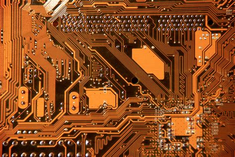
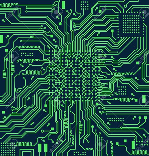
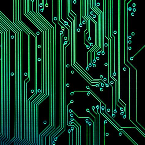
A circuit board, or PCB, is a flat board made of insulating materials, such as fiberglass or plastic, with conductive pathways etched onto its surface. These pathways, called traces, connect various electronic components like resistors, capacitors, and integrated circuits (ICs) to create a functional electronic circuit.
PCBs come in various sizes and shapes, depending on the device they are designed for. They can be single-sided (with components on one side), double-sided (with components on both sides), or multi-layered (with several layers of traces sandwiched between insulating layers).
Key Components of a PCB
A typical PCB consists of several key components:
- Substrate: The base material, usually made of fiberglass or plastic, that provides insulation and structural support.
- Copper Traces: Thin, conductive pathways etched onto the substrate that connect components.
- Solder Mask: A protective layer that covers the copper traces, preventing short circuits and oxidation.
- Silkscreen: Text and symbols printed on the PCB for easy identification of components and their placement.
- Vias: Small holes drilled through the board to connect traces on different layers.
- Electronic Components: Various parts, such as resistors, capacitors, and ICs, that are soldered onto the PCB to create the desired circuit.
How Does a PCB Work?
A PCB works by providing a platform for electronic components to be connected in a specific configuration to perform a desired function. The copper traces on the board act as wires, allowing electricity to flow between components.
When an electric current is applied to the PCB, it flows through the traces and components, following the designed circuit path. This flow of electricity enables the components to perform their intended functions, such as amplifying signals, processing data, or storing information.
PCB design Process
Creating a functional PCB involves several steps:
- Schematic Design: Engineers create a schematic diagram that represents the electronic circuit, showing how components are connected.
- PCB Layout: Using specialized software, designers convert the schematic into a physical layout, determining the placement of components and routing of traces.
- Fabrication: The designed PCB is manufactured using a combination of etching, drilling, and plating processes.
- Assembly: Electronic components are soldered onto the fabricated PCB, either manually or using automated machines.
- Testing: The assembled PCB is tested to ensure it functions as intended and meets the required specifications.
Types of PCBs
PCBs can be categorized based on their construction and the number of layers they have:
- Single-Sided PCB: A PCB with components and traces on only one side of the substrate. These are simple and inexpensive but have limited circuit complexity.
- Double-Sided PCB: A PCB with components and traces on both sides of the substrate, connected by vias. This allows for more complex circuits and better use of available space.
- Multi-Layer PCB: A PCB with multiple layers of traces sandwiched between insulating layers. These boards can accommodate highly complex circuits and are used in advanced electronic devices.
| PCB Type | Layers | Complexity | Cost | Common Applications |
|---|---|---|---|---|
| Single-Sided | 1 | Low | Low | Simple devices, hobby projects |
| Double-Sided | 2 | Medium | Medium | Modems, power supplies, amplifiers |
| Multi-Layer | 4+ | High | High | Smartphones, computers, servers |

Applications of PCBs
PCBs are used in virtually all electronic devices, from everyday consumer gadgets to advanced industrial equipment. Some common applications include:
- Consumer Electronics: Smartphones, laptops, tablets, televisions, gaming consoles, and wearable devices.
- Automotive Industry: Engine control units, infotainment systems, sensors, and electronic control modules.
- Medical Devices: Diagnostic equipment, monitoring systems, and implantable devices.
- Industrial Equipment: Automation systems, process control units, and power management devices.
- Aerospace and Defense: Avionics, radar systems, satellites, and military communication devices.
The widespread use of PCBs can be attributed to their numerous advantages, such as:
- Compact size and lightweight construction
- Reliable and consistent performance
- Reduced wiring and assembly time
- Lower production costs compared to point-to-point wiring
- Ease of maintenance and troubleshooting
Advances in PCB Technology
As electronic devices become more sophisticated and compact, PCB technology continues to evolve to meet the growing demands. Some of the latest advancements in PCB technology include:
- High-Density Interconnect (HDI) PCBs: These boards feature finer traces and smaller vias, allowing for higher component density and improved signal integrity.
- Flexible PCBs: Made from flexible materials like polyimide, these boards can bend and twist, making them suitable for wearable devices and applications with limited space.
- Rigid-Flex PCBs: A combination of rigid and flexible sections, these boards offer the benefits of both types, providing flexibility and stability where needed.
- 3D PCBs: These boards feature components mounted on multiple planes, allowing for more compact designs and shorter signal paths.
- Embedded PCBs: Components like capacitors and resistors are embedded within the board, further reducing the size and improving performance.
PCB Manufacturing Process
The manufacturing process for PCBs involves several steps, each requiring precision and expertise. The main stages of PCB manufacturing are:
- PCB Design: Creating the schematic and layout of the board using specialized software.
- Printing: Transferring the design onto the copper-clad substrate using a photoresist process.
- Etching: Removing unwanted copper from the substrate using chemicals, leaving only the desired traces.
- Drilling: Creating holes for vias and component leads using drill machines.
- Plating: Applying a thin layer of copper to the drilled holes to ensure electrical connectivity.
- Solder Mask Application: Covering the board with a protective layer, leaving only the areas where components will be soldered exposed.
- Silkscreen Printing: Adding text and symbols for component identification and orientation.
- Surface Finish: Applying a protective coating to the exposed copper to prevent oxidation and improve solderability.
- Electrical Testing: Verifying the board’s functionality and ensuring it meets the required specifications.
| Step | Process | Purpose |
|---|---|---|
| 1 | PCB Design | Create schematic and layout |
| 2 | Printing | Transfer design to substrate |
| 3 | Etching | Remove unwanted copper |
| 4 | Drilling | Create holes for vias and components |
| 5 | Plating | Ensure electrical connectivity |
| 6 | Solder Mask Application | Protect board and expose soldering areas |
| 7 | Silkscreen Printing | Add identification and orientation markings |
| 8 | Surface Finish | Prevent oxidation and improve solderability |
| 9 | Electrical Testing | Verify functionality and specifications |
Frequently Asked Questions (FAQ)
-
What is the difference between a PCB and a circuit board?
A PCB and a circuit board are essentially the same things. PCB is an acronym for Printed Circuit Board, which is the technical term for a circuit board. -
Can a PCB be repaired if damaged?
In most cases, a damaged PCB can be repaired by skilled technicians. However, the extent of the damage and the complexity of the board will determine the feasibility and cost-effectiveness of the repair. -
How long does a PCB last?
The lifespan of a PCB depends on various factors, such as the quality of materials, manufacturing process, and the environment in which it operates. Generally, a well-designed and manufactured PCB can last for several decades. -
Are PCBs environmentally friendly?
Modern PCBs are more environmentally friendly than their predecessors, thanks to the use of lead-free solder and the reduction of hazardous materials. However, proper disposal and recycling of PCBs are still crucial to minimize their environmental impact. -
What is the future of PCB technology?
As electronic devices continue to advance, PCB technology is expected to evolve, focusing on higher component density, improved signal integrity, and better thermal management. Emerging technologies like 5G, IoT, and AI will drive the development of more sophisticated and efficient PCBs.
Conclusion
In conclusion, a PCB, or Printed Circuit Board, is a fundamental component in modern electronics that provides a platform for connecting and integrating various electronic components. By understanding the basics of PCBs, their manufacturing process, and their applications, we can better appreciate the complex technology that powers our daily lives.
As PCB technology continues to advance, we can expect to see more compact, efficient, and sophisticated electronic devices in the future. From smartphones and laptops to medical devices and aerospace systems, PCBs will remain at the heart of the electronic world, enabling us to push the boundaries of what is possible.
Leave a Reply