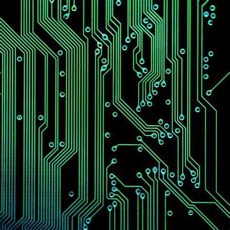
Introduction to PCBs and Circuit boards
In the world of software engineering, PCB stands for Printed Circuit Board. A PCB is a fundamental component in most electronic devices, serving as the foundation upon which various electronic components are mounted and interconnected. PCBs are essential in the design and development of software-driven hardware systems, as they provide a reliable and efficient means of connecting and integrating various components.
The Role of Circuit Boards in Software Engineering
Circuit boards, specifically PCBs, play a crucial role in software engineering by providing the physical platform that enables the integration of software with hardware components. Software engineers often work closely with hardware engineers and PCB designers to ensure that the software and hardware components of a system are seamlessly integrated and function as intended.
The Importance of Understanding PCBs for Software Engineers
While software engineers primarily focus on developing and maintaining software systems, understanding the basics of PCBs and their role in the overall system is essential. This knowledge helps software engineers:
- Communicate effectively with hardware engineers and PCB designers
- Design software that is compatible with the hardware components and limitations
- Optimize software performance based on the capabilities of the underlying hardware
- Troubleshoot issues that may arise due to hardware-software interactions
Types of PCBs Used in Software Engineering Projects
There are several types of PCBs used in software engineering projects, each with its own characteristics and applications. The most common types include:
1. Single-layer PCBs
Single-layer PCBs consist of a single conductive layer, usually made of copper, laminated onto an insulating substrate. These boards are the simplest and most cost-effective option, suitable for basic circuits and low-density designs.
| Characteristic | Description |
|---|---|
| Layers | One conductive layer |
| Cost | Low |
| Complexity | Simple |
| Applications | Basic circuits, low-density designs |
2. Double-layer PCBs
Double-layer PCBs have two conductive layers, one on each side of the insulating substrate. These boards offer more design flexibility and higher component density compared to single-layer PCBs. They are commonly used in more complex circuits and designs.
| Characteristic | Description |
|---|---|
| Layers | Two conductive layers |
| Cost | Moderate |
| Complexity | Medium |
| Applications | More complex circuits, higher density designs |
3. Multi-layer PCBs
Multi-layer PCBs consist of three or more conductive layers, separated by insulating layers. These boards are used in highly complex designs that require high component density and advanced signal routing. Multi-layer PCBs are commonly found in sophisticated electronic devices and systems.
| Characteristic | Description |
|---|---|
| Layers | Three or more conductive layers |
| Cost | High |
| Complexity | High |
| Applications | Highly complex designs, high-density components, advanced signal routing |
4. Flexible PCBs
Flexible PCBs, also known as flex circuits, are made using flexible insulating materials, such as polyimide, with thin conductive layers. These boards are designed to bend and flex, making them suitable for applications where flexibility and space constraints are critical factors.
| Characteristic | Description |
|---|---|
| Layers | Varies, can be single or multi-layer |
| Cost | High |
| Complexity | High |
| Applications | Flexible electronics, wearables, space-constrained designs |
PCB Design Considerations for Software Engineers
When working on projects that involve PCBs, software engineers should be aware of several key design considerations to ensure optimal system performance and reliability.
1. Component Selection and Placement
Selecting the appropriate components and placing them strategically on the PCB is crucial for ensuring proper functionality and minimizing signal interference. Software engineers should collaborate with hardware engineers to choose components that meet the system’s requirements and are compatible with the software being developed.
2. Signal Integrity and Routing
Maintaining signal integrity is essential for reliable communication between components on the PCB. Software engineers should be mindful of signal routing techniques, such as proper trace widths, spacing, and impedance matching, to minimize signal distortion and crosstalk.
3. Power Distribution and Grounding
Efficient power distribution and proper grounding are critical for stable system operation. Software engineers should work with hardware engineers to ensure that the PCB design incorporates appropriate power planes, decoupling capacitors, and ground planes to minimize noise and maintain a clean power supply.
4. Electromagnetic Compatibility (EMC)
EMC refers to the ability of electronic devices to function properly in the presence of electromagnetic interference (EMI) and to not emit excessive EMI that may disrupt other devices. Software engineers should be aware of EMC considerations and work with hardware engineers to implement techniques such as shielding, filtering, and proper grounding to ensure EMC compliance.
5. Thermal Management
Thermal management is crucial for maintaining the reliability and longevity of electronic components on a PCB. Software engineers should consider the power consumption and heat generation of the components they are using and work with hardware engineers to incorporate appropriate thermal management techniques, such as heatsinks, cooling fans, and thermal vias.

PCB Manufacturing Process Overview
Understanding the PCB manufacturing process can help software engineers appreciate the complexities involved in bringing their designs to life and make informed decisions when collaborating with hardware engineers and PCB manufacturers.
1. PCB Design and Layout
The PCB manufacturing process begins with the creation of a PCB design and layout using specialized software tools. The design includes the placement of components, routing of traces, and the definition of various layers and features.
2. PCB fabrication
Once the design is finalized, the PCB fabrication process begins. This process involves several steps, including:
a. Substrate preparation: The insulating substrate material is cut to size and cleaned.
b. Copper lamination: Thin layers of copper are laminated onto the substrate.
c. Photoresist application: A light-sensitive material called photoresist is applied to the copper layers.
d. Exposure and development: The photoresist is exposed to light through a photomask, which hardens the exposed areas. The unexposed areas are then removed during the development process.
e. Etching: The exposed copper is removed using a chemical etching process, leaving only the desired circuit patterns.
f. Drilling: Holes are drilled through the board to accommodate component leads and vias.
g. Plating: The holes are plated with copper to create electrical connections between layers.
h. Solder mask application: A protective solder mask is applied to the board, leaving only the exposed pads for component soldering.
i. Silkscreen printing: Text and symbols are printed onto the board for component identification and assembly guidance.
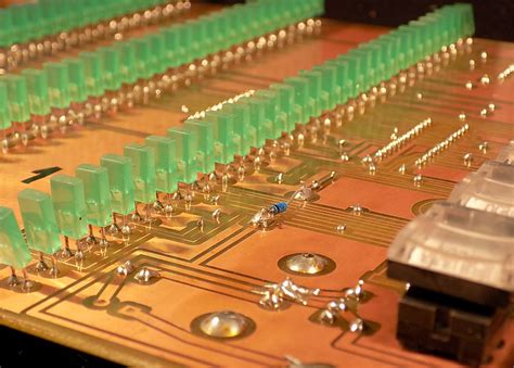
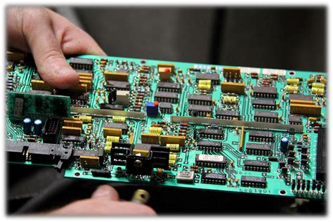
3. PCB Assembly
After the PCB fabrication process, the board undergoes assembly, where electronic components are mounted onto the board. This process can be done manually or using automated assembly machines, depending on the complexity and volume of the production run.
4. Testing and Quality Control
Once the PCB is assembled, it undergoes various testing and quality control procedures to ensure proper functionality and reliability. These tests may include:
a. Visual inspection: The assembled PCB is visually inspected for any defects or irregularities.
b. Automated Optical Inspection (AOI): An automated system scans the PCB for any missing or misplaced components, solder defects, or other issues.
c. In-Circuit Testing (ICT): The PCB is connected to a test fixture that verifies the proper functioning of individual components and circuits.
d. Functional testing: The PCB is tested under real-world operating conditions to ensure it performs as intended.
Best Practices for Software Engineers Working with PCBs
To ensure successful collaboration with hardware engineers and optimal system performance, software engineers should follow these best practices when working with PCBs:
1. Communicate and Collaborate Effectively
Maintain open and frequent communication with hardware engineers and PCB designers to ensure that software and hardware requirements are aligned and that any issues or constraints are addressed promptly.
2. Understand the Hardware Specifications
Familiarize yourself with the hardware specifications, including component datasheets, pin assignments, and communication protocols, to ensure that your software is compatible with the hardware and can take full advantage of its capabilities.
3. Optimize Software for Hardware Constraints
Be mindful of the hardware constraints, such as memory limitations, processing power, and power consumption, and optimize your software accordingly. This may involve using efficient algorithms, minimizing resource usage, and implementing power management techniques.
4. Test Early and Often
Regularly test your software on the target hardware platform to identify and resolve any issues early in the development process. This approach helps minimize the risk of costly redesigns and delays later in the project.
5. Stay Updated with Industry Trends and Best Practices
Keep abreast of the latest trends and best practices in PCB design and manufacturing, as well as advancements in software development methodologies and tools. This knowledge will help you make informed decisions and adapt to evolving project requirements.
Frequently Asked Questions (FAQ)
1. What is the difference between a PCB and a circuit board?
A PCB (Printed Circuit Board) is a specific type of circuit board that has conductive pathways printed or etched onto a non-conductive substrate. Circuit board is a more general term that encompasses various types of boards used to interconnect electronic components, including PCBs, breadboards, and prototyping boards.
2. How do software engineers typically interact with PCBs in their work?
Software engineers often work closely with hardware engineers and PCB designers to ensure that the software they develop is compatible with the hardware components and can effectively utilize the capabilities of the PCB. They may need to consider factors such as component selection, signal routing, and power management when designing software for embedded systems or devices that incorporate PCBs.
3. What are some common challenges software engineers face when working with PCBs?
Some common challenges include ensuring proper communication between software and hardware components, optimizing software performance within the constraints of the hardware, and troubleshooting issues that arise due to hardware-software interactions. Additionally, software engineers may need to adapt their development processes and testing methodologies to accommodate the unique requirements of working with PCBs.
4. How can software engineers improve their knowledge and skills related to PCBs?
Software engineers can improve their knowledge and skills related to PCBs by:
a. Collaborating closely with hardware engineers and PCB designers
b. Attending workshops, seminars, or courses focused on PCB design and manufacturing
c. Reading technical documentation, datasheets, and application notes for relevant components and technologies
d. Participating in online forums and communities dedicated to embedded systems and hardware-software co-design
e. Gaining hands-on experience by working on projects that involve PCBs and embedded systems
5. What are some emerging trends in PCB design and manufacturing that software engineers should be aware of?
Some emerging trends in PCB design and manufacturing include:
a. Increasing adoption of high-density interconnect (HDI) PCBs for miniaturization and improved performance
b. Growing use of flexible and rigid-flex PCBs for wearable devices and space-constrained applications
c. Advancements in materials science, such as the use of high-frequency and low-loss substrates for high-speed applications
d. Integration of embedded components and 3D packaging technologies for more compact and efficient designs
e. Increasing emphasis on sustainability and eco-friendly manufacturing processes
By staying informed about these trends, software engineers can better anticipate and adapt to the evolving requirements of PCB-based projects.
Conclusion
PCBs play a vital role in the world of software engineering, serving as the physical foundation upon which software-driven hardware systems are built. Understanding the basics of PCBs, their types, design considerations, and manufacturing processes is essential for software engineers to effectively collaborate with hardware engineers and create reliable, high-performance systems.
By following best practices, such as effective communication, understanding hardware specifications, optimizing software for hardware constraints, and staying updated with industry trends, software engineers can successfully navigate the challenges and opportunities presented by working with PCBs.
As technology continues to advance, the importance of PCBs in software engineering projects is likely to grow, making it increasingly critical for software engineers to have a solid understanding of these essential components. By embracing this knowledge and adapting to the evolving landscape of PCB design and manufacturing, software engineers can position themselves for success in the ever-changing world of technology.
Leave a Reply