History of the Printed Circuit Board
The printed circuit board has evolved over the past century to become an essential component in electronics manufacturing:
- 1903 – German inventor Albert Hanson described flat foil conductors laminated to an insulating board in multiple layers.
- 1927 – Charles Ducas of the United States submitted a patent application for a method of electroplating circuit patterns.
- 1936 – Paul Eisler of Austria patented a method for etching the conductive pattern, or circuits, on a layer of copper foil bonded to a non-conductive glass-epoxy board. This formed the basis of today’s printed circuit boards.
- 1943 – The United States began to use PCBs in proximity fuses during World War II.
- 1948 – The United States released the invention for commercial use.
- 1950s-1960s – PCBs developed through the addition of screen printing and photoengraving.
- 1970s-1980s – Hot air soldering and silk screen printing were popularized.
- 1980s-2000s – Surface mount technology was developed, PCB design software became widely available, and PCB manufacturing was largely automated.
Since the 2000s, further advancements have been made in materials, methods, and software to create the modern printed circuit board. Substrates such as aluminum, ceramic, and flexible materials are now used. Assembly methods have become more precise and efficient. PCB design software offers advanced simulation and testing capabilities.
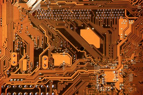
Anatomy of a Printed Circuit Board
The printed circuit board is composed of several key parts:
Substrate
The base material of the PCB, which is usually fiberglass. This provides a sturdy board for the copper layer to adhere to. Other substrates include composite epoxy, Teflon, ceramic, and flexible materials like polyimide films.
Copper Layer
Thin copper foil is laminated to the substrate. The circuits are formed by removing unwanted copper, leaving only the desired copper traces. This can be done through etching, milling, laser printing, or silk screen printing methods.
Solder Mask
A thin lacquer-like layer of polymer that is applied on top of the copper layer. It is typically green in color but can come in other colors. This solder mask insulates the copper traces from accidental contact and protects the board from solder during the assembly process.
Silkscreen
The white text, numbers and symbols printed onto the PCB. This is used to indicate component placement, test points, logos, version numbers, etc. Silkscreens are commonly printed via a silk screening process but can also be applied with ink-jet printers.
Solder Paste
Before components are mounted on boards with Surface Mount Technology (SMT), solder paste is applied to the solder pads via stencil printing. This paste contains tiny balls of solder suspended in flux. During reflow soldering, this paste melts to form soldered joints.
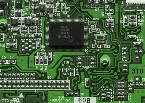
Components
The functional parts mounted on the PCB, such as integrated circuit (IC) chips, capacitors, resistors, etc. Through-hole components are inserted into holes drilled in the board and soldered in place. Surface mount components are placed on top of the board and soldered.
Types of Printed Circuit Boards
Printed circuit boards come in a variety of types suited for different applications:
Single-Sided PCB
These have one layer of substrate made of rigid laminate material. One side has a thin layer of metal, like copper, which is etched away to leave the circuit pattern on the board. Used for simple circuits.
Double-Sided PCB
These have a substrate with metal on both sides. Circuits on either side are connected with vias (holes drilled through the board). More complex circuits can be routed than single-sided boards.
Multi-Layer PCB
These contain more than two layers. The board consists of alternating layers of substrate material and copper. The layers are connected with vias. Used for very complex circuits.
Rigid PCB
These are the most common type, consisting of a rigid substrate material. They offer mechanical support to the components. Rigid PCBs cannot be bent or flexed.
Flexible PCB
Made with flexible high-temperature plastic, these can be bent and shaped to fit into limited spaces. They are lightweight and offer greater vibration resistance. Often used for circuitry in printers, cameras, and small electronics.
Rigid-Flex PCB
A combination of rigid and flexible circuit boards. Multiple layers of flexible circuit substrates are attached to one or more rigid boards externally or internally depending on design requirements. Used in aerospace and military applications.

PCB Design Software
PCB design software is used to layout the circuit pattern of conductors, passive components, and logic elements on the board. The designer must choose an optimal placement of components and routing of traces to create a PCB that is functional, efficient, and cost-effective.
Popular PCB design software includes:
- Altium Designer
- OrCAD
- EAGLE
- KiCad
- Fusion 360
These software packages offer schematic capture, component placement, and routing tools. Many also include simulation tools, manufacturer part information, and generate manufacturing output files.
PCB design software has made the printed circuit board design process more efficient and accessible. Designers can quickly create and revise PCB layouts. Simulations allow testing before physical prototyping. Generating manufacturing files is automated.
PCB Manufacturing Process
Once the PCB is designed, it must be manufactured. The PCB manufacturing process typically involves the following steps:
-
Material Selection – The appropriate substrate material is selected based on the intended application (standard FR-4, high-frequency, flexible, etc.)
-
Imaging – The circuit pattern is printed onto the substrate photoresist or resist ink.
-
Etching – The unwanted copper is chemically removed, leaving only the desired circuits.
-
Drilling – Holes are drilled into the board to allow for component leads and vias.
-
Plating – The holes are plated with copper to connect the different layers.
-
Solder Mask Application – The solder mask is applied to protect the copper circuits.
-
Silkscreen – The component legends are printed onto the board.
-
Surface Finish – A surface finish, such as HASL (solder), immersion silver, immersion tin, or ENIG (gold), is applied to the exposed copper to prevent oxidation.
-
Electrical Test – The board is tested to ensure no manufacturing defects are present.
-
Component Assembly – The components are mounted onto the board either through manual soldering, wave soldering (for through-hole components), or solder paste and reflow (for surface-mount components).
Many PCB manufacturers offer turnkey services that handle the entire process from design through component procurement and final assembly. Rapid prototyping services can produce PCBs in as fast as 24 hours.
Applications of Printed Circuit Boards
Printed circuit boards are used in virtually all electronic devices. Some common applications include:
Consumer Electronics
Televisions, stereos, video game consoles, digital cameras, mobile phones, home appliances, etc. The miniaturization of PCBs has enabled increasingly small and sophisticated consumer gadgets.
Computers
Desktop computers, laptops, tablets, servers, and computer peripherals all contain PCBs. A computer motherboard is one of the most complex examples of a printed circuit board.
Medical Devices
Medical equipment like patient monitors, imaging systems, and implantable devices rely on high-reliability PCBs. Medical PCBs must meet strict standards for quality and traceability.
Automotive
Modern vehicles contain dozens of PCBs for everything from the engine control unit to the entertainment system. Automotive PCBs must be designed to withstand vibration, temperature extremes, and long lifetimes.
Industrial
Industrial control systems, process controllers, robotics, and automation equipment use PCBs designed for reliability in harsh environments. Many industrial PCBs use surface coatings to protect against moisture, chemicals, and abrasion.
Aerospace and Defense
Avionics, radar systems, and control systems rely on advanced PCBs. PCBs for aerospace and military applications often use specialized materials like polyimide and require extensive qualification testing.
IoT Devices
The proliferation of the Internet of Things has driven demand for miniature, wireless-enabled PCBs. IoT device PCBs combine sensors, processors, and wireless connectivity into increasingly small form factors.
As electronics continue to become more integrated into all aspects of life, the applications for printed circuit boards will continue to expand. Emerging applications in wearable devices, smart homes, and autonomous vehicles will drive new innovations in PCB materials, manufacturing, and design.
Frequently Asked Questions
What is the difference between PCB and PCBA?
PCB stands for printed circuit board, which is the bare board with copper traces. PCBA stands for printed circuit board assembly, which is the completed board with components soldered on.
Are PCBs recyclable?
Yes, PCBs contain valuable metals like gold, silver, and copper that can be recovered through recycling processes. However, PCBs also contain hazardous materials like lead and brominated flame retardants that must be properly handled during recycling.
What is the most common PCB material?
FR-4 (Flame Retardant 4) is the most common base material for rigid PCBs. It is a glass-reinforced epoxy laminate that offers good insulation properties and mechanical strength.
How much does a printed circuit board cost?
The cost of a PCB depends on many factors such as the size, number of layers, materials, surface finishes, and quantity. Simple 2-layer PCBs can cost less than $1 each in volume, while complex multi-layer boards can cost hundreds of dollars each. Setup and tooling fees can add to the cost for low-volume production.
What is the lifespan of a PCB?
The lifespan of a PCB depends on the materials, manufacturing quality, and operating environment. Consumer-grade PCBs are often rated for a few years of use, while industrial and military-grade PCBs can last for decades. Factors like temperature, humidity, vibration, and power loads impact the lifespan.
In conclusion, the printed circuit board is a foundational component of modern electronics. Understanding what a PCB is, how it is made, and how it is used is essential for anyone involved in electronics design or manufacturing. As PCB technology continues to evolve, so too will the capabilities of the electronic devices that rely on them.
Leave a Reply