What is PCB Fabrication?
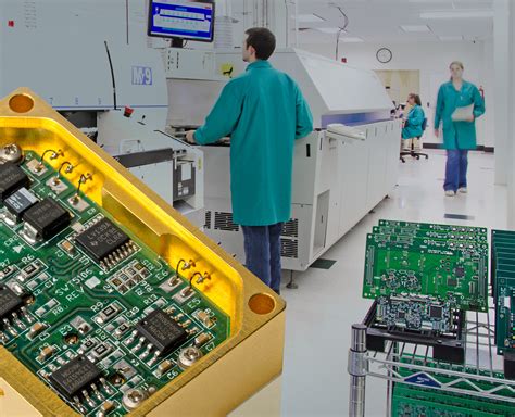
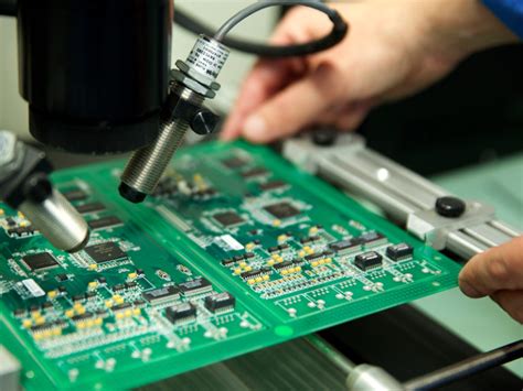
PCB fabrication is the process of creating a printed circuit board from a design layout. It involves a series of steps that transform a raw substrate material, typically a copper-clad laminate, into a functional PCB with conductive traces, pads, and other features. The fabrication process requires high precision, strict quality control, and adherence to industry standards to ensure the reliability and performance of the resulting PCBs.
The PCB Fabrication Process
The PCB fabrication process can be broken down into several key stages, each of which plays a critical role in the creation of a high-quality PCB. Let’s explore these stages in detail.
1. Design and Preparation
The PCB fabrication process begins with the design and preparation of the PCB layout. This stage involves the following steps:
1.1 Schematic Design
The first step in PCB design is creating a schematic diagram that represents the electrical connections and components of the circuit. The schematic is developed using Electronic Design Automation (EDA) software, which allows engineers to capture the logical design of the circuit.
1.2 PCB Layout Design
Once the schematic is complete, the next step is to create the physical layout of the PCB. This involves determining the placement of components, routing the conductive traces, and defining the board dimensions and layer stackup. The layout design must adhere to various design rules and constraints to ensure manufacturability and signal integrity.
1.3 Design Rule Check (DRC)
Before proceeding to fabrication, the PCB layout undergoes a Design Rule Check (DRC) to verify that it meets the manufacturer’s specifications and industry standards. The DRC helps identify and resolve any potential issues, such as trace width violations, clearance errors, or component placement conflicts.
1.4 Gerber File Generation
After the PCB layout is finalized and passes the DRC, the design files are converted into Gerber format. Gerber files are the industry standard for PCB fabrication and contain all the necessary information for each layer of the PCB, including copper traces, solder mask, silkscreen, and drill data.
2. Material Selection and Preparation
The selection and preparation of the PCB substrate material is a critical step in the fabrication process. The most commonly used substrate is FR-4, a glass-reinforced epoxy laminate. However, other materials like polyimide, ceramic, or metal-core PCBs may be used depending on the specific application requirements.
2.1 Copper Clad Laminate
The starting material for PCB fabrication is a copper-clad laminate, which consists of a thin layer of copper foil bonded to one or both sides of the substrate material. The thickness of the copper foil can vary depending on the desired current carrying capacity and signal integrity requirements.
2.2 Cutting and Drilling
The copper-clad laminate is cut to the required board dimensions using precision cutting machines. Holes are then drilled through the laminate at the locations specified in the drill data file. These holes serve as vias for interconnecting different layers of the PCB or as mounting holes for components.
3. Patterning and Etching
The patterning and etching stage is where the conductive traces and pads are formed on the PCB. This stage involves the following steps:
3.1 Photoresist Application
A photosensitive material called photoresist is applied to the copper surface of the laminate. The photoresist can be either liquid or dry film and is typically applied using a laminator or screen printing process.
3.2 Exposure and Development
The PCB panel with the applied photoresist is then exposed to UV light through a photomask or direct imaging process. The photomask contains the negative image of the copper pattern for each layer of the PCB. The UV light hardens the exposed areas of the photoresist, while the unexposed areas remain soluble.
After exposure, the PCB panel is developed in a chemical solution that removes the soluble photoresist, leaving the hardened photoresist in place. This process creates a protective mask over the areas where the copper traces and pads will remain.
3.3 Etching
The exposed copper areas not protected by the hardened photoresist are then etched away using a chemical etching process. The most common etchant used is acidified cupric chloride or ammoniacal copper chloride. The etching process removes the unwanted copper, leaving behind the desired conductive pattern.
3.4 Photoresist Stripping
After etching, the remaining hardened photoresist is stripped away using a chemical stripping solution, revealing the final copper pattern on the PCB.
4. Lamination and Drilling
For multi-layer PCBs, the individual patterned layers need to be laminated together to form a single board. This stage involves the following steps:
4.1 Layer Alignment
The patterned layers are aligned and stacked in the proper sequence according to the PCB design. Prepreg, a pre-impregnated bonding material, is placed between the layers to provide insulation and adhesion during lamination.
4.2 Lamination
The stacked layers and prepreg are placed in a lamination press, where they are subjected to high pressure and temperature. The heat and pressure cause the prepreg to melt and bond the layers together, creating a solid multi-layer PCB.
4.3 Drilling
After lamination, additional holes are drilled through the multi-layer PCB as specified in the drill data file. These holes include vias for interconnecting the layers and component mounting holes.
5. Surface Finishes and Solder Mask
To protect the copper traces and pads from oxidation and enhance solderability, various surface finishes are applied to the PCB. Additionally, a solder mask is applied to insulate and protect the copper areas not intended for soldering.
5.1 Surface Finishes
Common surface finishes include:
- Hot Air Solder Leveling (HASL): A tin-lead alloy is applied to the copper surfaces and then leveled using hot air.
- Electroless Nickel Immersion Gold (ENIG): A thin layer of nickel is deposited on the copper, followed by a thin layer of gold.
- Immersion Silver: A thin layer of silver is chemically deposited on the copper surfaces.
- Immersion Tin: A thin layer of tin is chemically deposited on the copper surfaces.
5.2 Solder mask application
A solder mask is a polymer coating applied to the PCB surface to protect the copper traces and prevent solder bridging. The solder mask is typically applied using screen printing or photoimaging techniques and is available in various colors, with green being the most common.
6. Silkscreen and Final Finishing
The final stages of the PCB fabrication process involve applying the silkscreen and performing any necessary finishing steps.
6.1 Silkscreen Application
The silkscreen is a graphical overlay that provides text, logos, and component identification markings on the PCB surface. It is typically applied using a screen printing process with ink that contrasts with the solder mask color.
6.2 Final Finishing
After the silkscreen application, the PCB undergoes final finishing steps, such as:
- Electrical Testing: The PCB is tested for continuity, shorts, and opens to ensure electrical integrity.
- Visual Inspection: The PCB is visually inspected for any defects or anomalies.
- Surface Cleaning: The PCB surface is cleaned to remove any contaminants or residues.
- Packaging: The finished PCBs are packaged and prepared for shipment to the customer.

PCB Fabrication Considerations
When designing and fabricating PCBs, several key considerations must be taken into account to ensure the optimal performance and reliability of the final product. These considerations include:
1. Material Selection
The choice of PCB substrate material depends on factors such as the operating environment, thermal requirements, Dielectric Properties, and cost. FR-4 is the most common material for general-purpose PCBs, but other materials like polyimide, ceramic, or metal-core PCBs may be used for specific applications.
2. Layer Stackup
The layer stackup of a PCB refers to the arrangement and thickness of the conductive and insulating layers. Proper layer stackup design is crucial for maintaining signal integrity, controlling impedance, and minimizing crosstalk. The number of layers and their arrangement depend on the complexity of the circuit and the signal routing requirements.
3. Trace Width and Spacing
The width and spacing of the conductive traces on a PCB are critical for ensuring proper current carrying capacity and preventing signal interference. The trace width is determined by the required current carrying capacity, while the spacing between traces is governed by the voltage difference and the PCB manufacturing capabilities.
4. Via Design
Vias are the conductive pathways that interconnect different layers of a multi-layer PCB. Via design considerations include the via size, pad size, and via type (through-hole, blind, or buried). Proper via design helps ensure reliable interconnections and minimizes signal integrity issues.
5. Solder Mask and Silkscreen
The solder mask and silkscreen are important for protecting the PCB and providing clear markings for assembly and identification. The solder mask color and thickness should be chosen based on the application requirements and the desired visual appearance. The silkscreen should be legible and properly aligned with the underlying features.
6. Manufacturing Capabilities
PCB fabrication is subject to the capabilities and limitations of the manufacturing process. Designers must consider factors such as minimum feature sizes, hole sizes, aspect ratios, and tolerances when creating the PCB layout. Communication with the PCB manufacturer is essential to ensure that the design is compatible with their manufacturing capabilities.

Frequently Asked Questions (FAQ)
- What is the difference between a single-layer and multi-layer PCB?
A Single-Layer PCB has conductive traces on only one side of the substrate, while a multi-layer PCB has conductive traces on multiple layers that are interconnected using vias. Multi-layer PCBs offer higher component density, better signal integrity, and improved EMI/RFI shielding compared to single-layer PCBs.
- What is the purpose of the solder mask on a PCB?
The solder mask is a protective coating applied to the PCB surface that covers the copper traces and pads not intended for soldering. It serves several purposes, including:
– Preventing solder bridging between closely spaced pads
– Protecting the copper from oxidation and contamination
– Providing electrical insulation between conductive areas
– Enhancing the visual appearance of the PCB
- What are the common surface finishes used in PCB fabrication?
Common surface finishes used in PCB fabrication include:
– Hot Air Solder Leveling (HASL): A tin-lead alloy is applied to the copper surfaces and leveled using hot air.
– Electroless Nickel Immersion Gold (ENIG): A thin layer of nickel is deposited on the copper, followed by a thin layer of gold.
– Immersion Silver: A thin layer of silver is chemically deposited on the copper surfaces.
– Immersion Tin: A thin layer of tin is chemically deposited on the copper surfaces.
The choice of surface finish depends on factors such as solderability, shelf life, cost, and compatibility with the assembly process.
- What is the role of the Gerber files in PCB fabrication?
Gerber files are the industry standard format for conveying PCB design information to the fabrication process. They contain all the necessary data for each layer of the PCB, including:
– Copper traces and pads
– Solder mask openings
– Silkscreen markings
– Drill data
The Gerber files are used by the PCB manufacturer to create the photomasks or direct imaging data required for the patterning and etching process.
- What are the typical lead times for PCB fabrication?
The lead times for PCB fabrication can vary depending on factors such as the complexity of the design, the number of layers, the selected surface finish, and the manufacturing capacity of the PCB fabricator. Typical lead times range from a few days to several weeks, with the following general guidelines:
– Simple, single-layer PCBs: 1-3 days
– Double-layer PCBs: 3-5 days
– Multi-layer PCBs (4-8 layers): 7-10 days
– Complex, high-layer count PCBs (10+ layers): 2-3 weeks
Rush services may be available for faster turnaround times, but they often come at a premium cost.

Conclusion
The PCB fabrication process is a complex and precise endeavor that transforms a PCB design into a functional physical board. By understanding the various stages involved, from design and material preparation to patterning, etching, and finishing, designers can make informed decisions and optimize their PCB layouts for manufacturability and reliability.
Effective communication between the PCB designer and the fabricator is essential to ensure that the design is compatible with the manufacturing capabilities and meets the required specifications. By considering factors such as material selection, layer stackup, trace width and spacing, via design, and surface finishes, designers can create PCBs that meet the performance and reliability requirements of their applications.
As PCB technology continues to evolve, with increasing demands for miniaturization, high-speed signaling, and advanced packaging, the PCB fabrication process will continue to adapt and innovate to meet these challenges. By staying informed about the latest manufacturing techniques and design best practices, PCB designers can create cutting-edge products that push the boundaries of electronic innovation.
| PCB Fabrication Process Steps | Description |
|---|---|
| 1. Design and Preparation | – Schematic design – PCB layout design – Design Rule Check (DRC) – Gerber file generation |
| 2. Material Selection and Preparation | – Copper clad laminate selection – Cutting and drilling |
| 3. Patterning and Etching | – Photoresist application – Exposure and development – Etching – Photoresist stripping |
| 4. Lamination and Drilling | – Layer alignment – Lamination – Drilling |
| 5. Surface Finishes and Solder Mask | – Surface finish application (HASL, ENIG, Immersion Silver, Immersion Tin) – Solder mask application |
| 6. Silkscreen and Final Finishing | – Silkscreen application – Electrical testing – Visual inspection – Surface cleaning – Packaging |
By following these steps and considering the key factors involved in PCB fabrication, designers and manufacturers can collaborate effectively to create high-quality, reliable PCBs that meet the demands of modern electronic applications.

Leave a Reply