What are Microvias in PCBs?
Microvias are small holes drilled in a printed circuit board (PCB) that electrically connect different layers of the board. Unlike through-holes which go through the entire board, microvias only penetrate through a few layers. This allows for greater interconnection density and routing flexibility in high density PCB Designs.
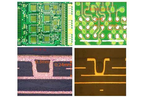
Microvia PCB Specifications and Dimensions
Typical microvias have the following dimensions:
| Dimension | Size Range |
|---|---|
| Diameter | 50-150 μm |
| Depth | 60-150 μm |
| Pad Size | 200-600 μm |
| Pitch | 200-1000 μm |
The small size of microvias enables designers to pack more interconnects in a given area compared to through-hole vias. This is essential for compact electronics packaging.
Microvia Aspect Ratio
The aspect ratio is the ratio of a microvia’s depth to its diameter. Standard microvias have an aspect ratio between 0.5:1 and 1:1. Higher aspect ratios up to 2.5:1 are possible but more challenging to reliably manufacture.
How are Microvias Formed?
Several methods are used to create microvias in PCBs:
Laser Drilling
Laser drilling is the most common method to form microvias. A focused laser beam ablates the dielectric material to create the hole. CO2 lasers (9.3-10.6 μm) and UV lasers (355 nm) are typically used.
Advantages of laser drilling include:
– High precision and small via sizes
– Fast drilling speed
– No contact with PCB surface
– Minimal stress on the board
Mechanical Drilling
Mechanical drills with small diameter bits (50-200 μm) can also be used to create microvias. However, mechanical drilling is slower and less precise than laser drilling. The contact with the PCB can also cause mechanical stress.
Photo-definition
Photovias are formed by selectively exposing a photosensitive dielectric layer to create openings. This method has high precision but requires specific photoimageable materials and processing steps.
Microvia Reliability Concerns
While microvias enable high density PCB designs, they also present some reliability challenges that designers need to consider:
Thermal Cycling Fatigue
Thermal stresses from coefficient of thermal expansion (CTE) mismatches can cause fatigue cracking in microvias, especially under repeated thermal cycling. Stacked microvias are particularly susceptible. Using larger via capture pads, adding anchors, and limiting stacked microvias can improve thermal cycling reliability.
Outgassing and Fluid Pressure
During reflow soldering, any moisture trapped in the PCB can vaporize and cause delamination or blowholes around microvias. Proper PCB baking before reflow and using vacuum lamination can mitigate this issue. Limiting the microvia aspect ratio also helps.
Chemical Contamination
Microvias can trap chemical contaminants from processing that corrode the metal and cause interconnect failures. Thorough cleaning and using a microvia fill material prevents contamination.

HDI PCB Design Guidelines for Microvias
To ensure reliable microvias in high density interconnect (HDI) PCB designs, follow these guidelines:
- Limit stacked microvias to 2-3 levels to minimize stress concentration
- Use larger via capture pads (>150 μm) for improved registration
- Specify a minimum microvia-to-microvia spacing >250 μm
- Keep microvia aspect ratios <1:1 when possible
- Avoid staggered microvias which cause uneven dielectric thickness
- Use microvia fill material to prevent contamination
- Follow manufacturer design rules and tolerances for specific processes
Frequently Asked Questions
What is the minimum size of a microvia?
The minimum diameter of a microvia depends on the PCB fabricator’s capabilities, but is typically around 50 μm. Anything smaller becomes difficult to produce reliably.
How many microvias can be stacked on top of each other?
Most PCB manufacturers can stack up to 2-3 blind microvias on top of each other. Stacking more levels is possible but increases the risk of defects and failures. Buried stacked microvias are generally limited to 2 levels.
What materials are compatible with microvias?
Microvias can be formed in most standard PCB dielectrics including FR-4, polyimide, and high-frequency laminates. Some specialized materials like PTFE require different processing. The dielectric material must be compatible with the microvia formation method used (laser drilling, photo-definition, etc.).
How much do microvias add to PCB Cost?
Adding microvias to a PCB design increases the cost due to the additional processing steps required. In general, expect a 20-30% cost adder for designs with a single level of microvias. Each additional microvia level can add another 10-20% to the cost. The exact cost impact varies by PCB fabricator, design complexity, and volume.
Are microvias necessary for every PCB design?
No, microvias are not required for every PCB. They are most commonly used in high density designs that have fine-pitch components, large pin-count chips, or limited space. Simpler PCBs can often be routed using only through-hole vias. However, microvias provide valuable flexibility for dense area breakouts and complex routing even on otherwise low-density boards.
Conclusion
Microvias are a key enabling technology for high density PCB designs. By understanding the capabilities, trade-offs, and design guidelines for using microvias, engineers can take full advantage of their benefits while ensuring a reliable and manufacturable design.
When considering microvias, work closely with your PCB manufacturer to understand their specific processes, tolerances, and recommendations. Following best practices and balancing the electrical, thermal, and mechanical requirements will result in a successful HDI design.
Leave a Reply