Understanding PCB Cost Drivers
When it comes to printed circuit board (PCB) design, cost is always a primary consideration. A thorough understanding of the factors that drive PCB cost is essential for making informed decisions during the design process. Some of the key PCB cost drivers include:
Material Selection
The choice of materials used in PCB fabrication can significantly impact the overall cost. Factors to consider include:
- Substrate material (e.g., FR-4, Rogers, Polyimide)
- Copper weight and thickness
- Surface finish (e.g., HASL, ENIG, OSP)
| Material | Relative Cost |
|---|---|
| FR-4 | Low |
| Rogers | High |
| Polyimide | Medium |
Board Size and Complexity
The size and complexity of the PCB design directly influence the manufacturing cost. Consider the following:
- Board dimensions
- Number of layers
- Minimum trace width and spacing
- Via size and density
| Board Size | Relative Cost |
|---|---|
| Small | Low |
| Medium | Medium |
| Large | High |
Component Selection
The choice of components used in the PCB assembly also plays a significant role in the overall cost. Key factors include:
- Component package types (e.g., SMD, through-hole)
- Component availability and lead times
- Component pricing and minimum order quantities
| Component Package | Relative Cost |
|---|---|
| SMD | Low |
| Through-hole | Medium |
| BGA | High |
Strategies for Reducing PCB Cost
With a clear understanding of the cost drivers, PCB designers can employ various strategies to minimize expenses without compromising functionality or reliability. Some effective cost-reduction strategies include:
Design for Manufacturability (DFM)
Incorporating DFM principles into the PCB design process can help minimize manufacturing challenges and reduce costs. Key DFM considerations include:
- Adhering to recommended trace width and spacing guidelines
- Minimizing the number of unique hole sizes
- Avoiding unnecessary complexity in board shape and routing
Component Standardization
Standardizing components across multiple designs can lead to significant cost savings by:
- Reducing the number of unique parts to manage
- Enabling bulk purchasing at discounted prices
- Minimizing the risk of obsolescence
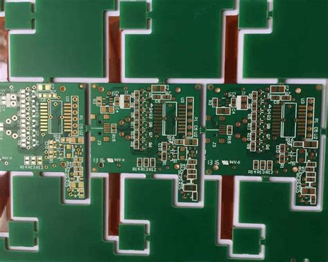
Panelization
Designing PCBs to be manufactured in panels can reduce costs by:
- Maximizing material utilization
- Reducing handling and setup time
- Enabling more efficient assembly processes

Case Study: Implementing Cost-Saving Strategies
To illustrate the potential impact of cost-saving strategies, let’s consider a hypothetical case study involving the redesign of a medium-complexity PCB.
Original Design
- Board size: 100 mm x 80 mm
- Number of layers: 6
- Unique components: 150
- Estimated cost per board: $25
Redesigned with Cost-Saving Strategies
- Board size: 90 mm x 70 mm (10% reduction)
- Number of layers: 4 (33% reduction)
- Unique components: 120 (20% reduction)
- Estimated cost per board: $18 (28% reduction)
By implementing cost-saving strategies such as design optimization, component standardization, and panelization, the redesigned PCB achieved a significant 28% cost reduction without compromising functionality or reliability.

Future Trends in PCB Cost Reduction
As technology advances and market demands evolve, new opportunities for PCB cost reduction are emerging. Some notable trends include:
Additive Manufacturing
Additive manufacturing techniques, such as 3D printing, offer the potential for more efficient and cost-effective PCB fabrication. Benefits include:
- Reduced material waste
- Faster prototyping and iteration
- Increased design flexibility
Embedded Components
Integrating passive components directly into the PCB substrate can lead to cost savings by:
- Reducing the number of discrete components
- Minimizing assembly complexity
- Enabling more compact board designs
Automated Design Tools
The development of advanced, AI-driven PCB design tools can help designers quickly identify and implement cost-saving opportunities by:
- Analyzing design data to suggest optimizations
- Flagging potential manufacturability issues
- Streamlining the design process through automation

Conclusion
PCB cost reduction is an ongoing priority for designers and manufacturers alike. By understanding the key cost drivers, implementing proven cost-saving strategies, and staying informed about emerging trends, PCB designers can create high-quality, cost-effective solutions that meet the evolving needs of the electronics industry.
Frequently Asked Questions (FAQ)
1. What is the most significant factor in determining PCB cost?
The most significant factor in determining PCB cost is typically the complexity of the board design, which encompasses aspects such as board size, number of layers, and component density.
2. How can component standardization help reduce PCB cost?
Component standardization can help reduce PCB cost by minimizing the number of unique parts to manage, enabling bulk purchasing at discounted prices, and reducing the risk of obsolescence.
3. What is Design for Manufacturability (DFM), and how does it impact PCB cost?
Design for Manufacturability (DFM) is a set of principles and practices aimed at optimizing PCB designs for efficient and cost-effective manufacturing. By incorporating DFM considerations, designers can minimize manufacturing challenges and reduce overall costs.
4. How can additive manufacturing techniques, such as 3D printing, help reduce PCB cost?
Additive manufacturing techniques, like 3D printing, can help reduce PCB cost by minimizing material waste, enabling faster prototyping and iteration, and allowing for increased design flexibility.
5. What role do automated design tools play in PCB cost reduction?
Automated design tools, particularly those driven by AI, can help designers quickly identify and implement cost-saving opportunities by analyzing design data, suggesting optimizations, flagging potential manufacturability issues, and streamlining the design process through automation.

Leave a Reply