Introduction to PCB
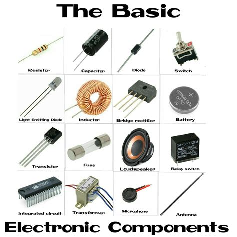
PCB stands for Printed Circuit Board, which is a fundamental component in modern electronic devices. It is a flat board made of insulating materials, such as fiberglass or composite epoxy, with conductive copper traces etched onto its surface. These traces connect various electronic components, such as resistors, capacitors, and integrated circuits, to form a complete electrical circuit.
PCBs have revolutionized the electronics industry by providing a reliable, compact, and cost-effective way to assemble electronic circuits. They are used in a wide range of applications, from simple consumer electronics to complex industrial equipment and aerospace systems.
History of PCB
The concept of PCBs dates back to the early 20th century when inventors began experimenting with ways to simplify the wiring of electronic devices. In 1936, Austrian engineer Paul Eisler invented the first printed circuit as part of a radio set. However, it wasn’t until the 1950s that PCBs became widely used in the electronics industry.
During World War II, the U.S. military heavily invested in the development of PCBs to improve the reliability and reduce the size of electronic equipment used in warfare. After the war, the technology became more accessible and affordable, leading to its adoption in consumer electronics.
Types of PCBs
There are several types of PCBs, each with its own unique characteristics and applications. The most common types include:
-
Single-layer PCB: These have conductive traces on only one side of the board and are used in simple, low-cost electronic devices.
-
Double-layer PCB: With conductive traces on both sides of the board, these offer more design flexibility and are used in more complex devices.
-
Multi-layer PCB: These consist of multiple layers of conductive traces separated by insulating material, allowing for even greater design complexity and higher component density. They are used in advanced electronic systems, such as smartphones, computers, and medical equipment.
-
Flexible PCB: Made from flexible materials, these can be bent or shaped to fit into tight spaces or conform to unique product designs.
-
Rigid-Flex PCB: A combination of rigid and flexible PCBs, these offer the benefits of both types and are used in applications that require both stability and flexibility.
PCB Manufacturing Process
The PCB manufacturing process involves several steps, each requiring precision and attention to detail to ensure the quality and reliability of the final product.
PCB design
The first step in the PCB manufacturing process is the design phase. This involves creating a schematic diagram of the electronic circuit and a layout of the PCB using specialized software. The designer must consider factors such as component placement, trace width and spacing, and power distribution to ensure optimal performance and manufacturability.
PCB fabrication
Once the design is finalized, the PCB fabrication process begins. This typically involves the following steps:
-
Material preparation: The raw PCB material, usually a copper-clad laminate, is cut to the desired size and shape.
-
Drilling: Holes are drilled into the board to accommodate through-hole components and provide electrical connections between layers.
-
Patterning: The copper traces are created on the board using a photolithographic process. This involves applying a light-sensitive resist to the copper, exposing it to UV light through a patterned mask, and then etching away the unwanted copper.
-
Lamination: For multi-layer PCBs, the individual layers are aligned and bonded together under high pressure and temperature.
-
Surface finishing: A protective coating, such as solder mask or silkscreen, is applied to the board to insulate the copper traces and prevent oxidation.
PCB Assembly
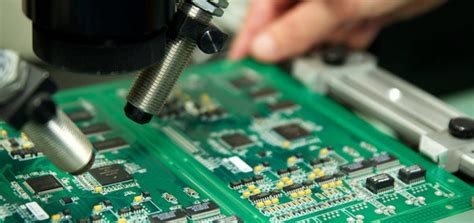
After the PCB fabrication is complete, the electronic components are attached to the board through a process called PCB assembly. This can be done manually for low-volume production or using automated equipment for high-volume manufacturing.
The two main methods of PCB assembly are:
-
Through-hole technology (THT): Components with long leads are inserted into the holes drilled in the PCB and soldered in place.
-
Surface mount technology (SMT): Components are placed directly onto the surface of the PCB and soldered using a reflow oven.
Advantages of Using PCBs
PCBs offer several advantages over traditional point-to-point wiring methods, making them essential in modern electronics:
-
Compact size: PCBs allow for the miniaturization of electronic devices by enabling high component density and efficient use of space.
-
Reliability: The robust construction and precise manufacturing process of PCBs ensure consistent performance and reduce the risk of electrical failures.
-
Cost-effective: Mass production of PCBs is relatively inexpensive, making them a cost-effective solution for large-scale electronic manufacturing.
-
Reproducibility: PCBs enable the creation of identical electronic circuits, ensuring consistency across multiple units of the same product.
-
Design flexibility: PCBs can be customized to suit specific application requirements, allowing for the integration of various components and features.

Applications of PCBs
PCBs are used in virtually every electronic device, from everyday consumer products to advanced industrial systems. Some common applications include:
-
Consumer electronics: Smartphones, tablets, laptops, televisions, and home appliances.
-
Automotive industry: Engine control units, infotainment systems, and advanced driver assistance systems (ADAS).
-
Medical devices: Diagnostic equipment, patient monitoring systems, and implantable devices.
-
Aerospace and defense: Avionics, radar systems, and satellite communication equipment.
-
Industrial automation: Process control systems, robotics, and power electronics.
Future of PCB Technology
As electronic devices continue to evolve and become more sophisticated, PCB technology must adapt to meet new challenges and demands. Some of the emerging trends in PCB design and manufacturing include:
-
High-density interconnect (HDI): HDI PCBs feature finer traces and smaller vias, enabling even greater component density and miniaturization.
-
Embedded components: Passive components, such as resistors and capacitors, can be embedded within the layers of a PCB, saving space and improving performance.
-
3D printing: Additive manufacturing techniques, such as 3D printing, are being explored as a way to create complex PCB Structures and reduce production time and costs.
-
Advanced materials: New PCB materials, such as high-frequency laminates and thermally conductive substrates, are being developed to meet the demands of emerging applications, such as 5G wireless and power electronics.
Frequently Asked Questions (FAQ)
- What is the difference between a PCB and a printed wiring board (PWB)?
-
A PWB is a more general term that includes both PCBs and other types of boards with printed conductors. PCBs are a specific type of PWB that have copper traces etched onto a non-conductive substrate.
-
Can PCBs be recycled?
-
Yes, PCBs can be recycled to recover valuable materials, such as copper and precious metals. However, the recycling process is complex and requires specialized facilities to ensure proper handling of potentially hazardous substances.
-
How long do PCBs last?
-
The lifespan of a PCB depends on various factors, such as the quality of materials, manufacturing process, and operating environment. With proper design and manufacturing, PCBs can last for decades in normal operating conditions.
-
What is the difference between a single-sided and double-sided PCB?
-
A single-sided PCB has conductive traces on only one side of the board, while a double-sided PCB has traces on both sides. Double-sided PCBs offer more design flexibility and higher component density compared to single-sided PCBs.
-
What is the role of solder mask on a PCB?
- Solder mask is a protective coating applied to the copper traces on a PCB. It serves to insulate the traces, prevent short circuits, and protect against oxidation. Solder mask also provides a visual contrast that aids in the assembly process.
Conclusion
PCBs are essential components in modern electronic devices, providing a reliable, compact, and cost-effective way to assemble electronic circuits. The technology has evolved significantly since its inception, with advancements in materials, manufacturing processes, and design software. Today, PCBs are used in a wide range of applications, from consumer electronics to industrial automation and aerospace systems. As electronic devices continue to become more complex and sophisticated, PCB technology will continue to adapt and innovate to meet the demands of the future.
| Parameter | Value |
|---|---|
| PCB Type | Single-layer, Double-layer, Multi-layer, Flexible, Rigid-Flex |
| Material | FR-4, High-frequency laminates, Thermally conductive substrates |
| Manufacturing Process | Design, Fabrication (Material preparation, Drilling, Patterning, Lamination, Surface finishing), Assembly (THT, SMT) |
| Applications | Consumer electronics, Automotive, Medical devices, Aerospace and defense, Industrial automation |
| Future Trends | High-density interconnect (HDI), Embedded components, 3D printing, Advanced materials |
Leave a Reply