Introduction to PCB-PTH Technology
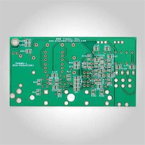
Printed Circuit Board (PCB) design involves various techniques and technologies to create reliable and efficient electronic circuits. One such technology is Plated Through Hole (PTH), which has been widely used in the PCB industry for decades. PTH is a method of creating electrical connections between different layers of a PCB by drilling holes through the board and plating them with a conductive material, typically copper.
In this article, we will explore the benefits of using PTH technology in PCB design, its applications, and some best practices for implementing it effectively.
What is Plated Through Hole (PTH) Technology?
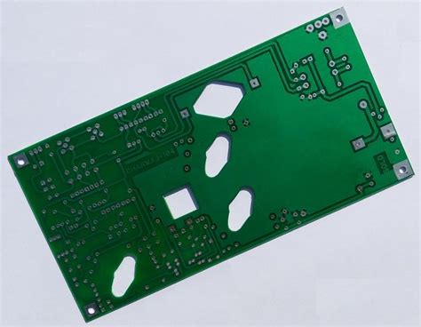
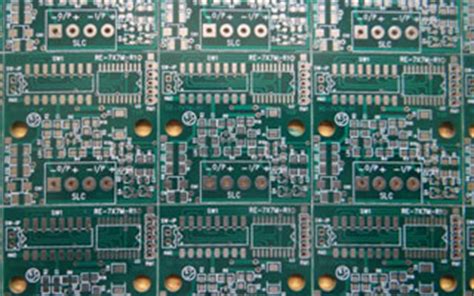
PTH is a process used in PCB manufacturing where holes are drilled through the board and then plated with a conductive material, usually copper, to create electrical connections between different layers of the PCB. The plating process involves depositing a thin layer of copper on the walls of the drilled holes, ensuring a reliable electrical connection between the layers.
The PTH process typically involves the following steps:
- Drilling holes through the PCB using a CNC machine or laser
- Cleaning and deburring the holes to remove any debris
- Applying a thin layer of copper to the walls of the holes through electroless plating
- Electroplating additional copper to increase the thickness of the conductive layer
- Applying a final finish, such as solder mask or surface finish, to protect the copper and enhance solderability

Benefits of Using PTH in PCB Design
Improved Mechanical Strength
One of the primary benefits of using PTH in PCB design is the improved mechanical strength it provides. The plated holes act as rivets, holding the layers of the PCB together and preventing delamination. This is particularly important in applications where the PCB is subject to vibration, shock, or thermal stress.
Enhanced Electrical Conductivity
PTH ensures a reliable electrical connection between the layers of the PCB, reducing the risk of signal loss or interference. The plated holes provide a low-resistance path for electrical signals to travel between layers, improving the overall performance of the circuit.
Increased Current Carrying Capacity
The plated holes in a PTH PCB can carry higher currents compared to surface-mounted connections. This is because the plated holes have a larger cross-sectional area, allowing them to handle higher current densities without overheating or suffering from voltage drop.
Better Heat Dissipation
PTH technology also helps in better heat dissipation from the components mounted on the PCB. The plated holes act as thermal vias, conducting heat away from the components and into the PCB substrate, which can then dissipate the heat to the environment.
Compatibility with Through-Hole Components
PTH is essential for mounting through-hole components, such as connectors, switches, and some types of capacitors and resistors. These components have leads that are inserted into the plated holes and soldered in place, ensuring a secure mechanical and electrical connection.

Applications of PTH in PCB Design
PTH technology finds applications in various industries and product categories. Some common applications include:
Consumer Electronics
PTH is widely used in consumer electronics, such as smartphones, tablets, laptops, and wearables. These devices often require high-density PCBs with multiple layers and a mix of surface-mounted and through-hole components.
Automotive Electronics
The automotive industry relies heavily on PTH PCBs for their reliability and durability. Automotive electronics, such as engine control units, sensors, and infotainment systems, are subject to harsh environmental conditions, including temperature extremes, vibration, and moisture. PTH helps ensure the integrity of the electrical connections in these challenging conditions.
Industrial Control Systems
Industrial control systems, such as programmable logic controllers (PLCs), human-machine interfaces (HMIs), and supervisory control and data acquisition (SCADA) systems, often use PTH PCBs for their robustness and reliability. These systems are critical for controlling and monitoring industrial processes and must function reliably in demanding environments.
Medical Devices
Medical devices, such as patient monitors, diagnostic equipment, and implantable devices, require high-reliability PCBs that can withstand sterilization processes and operate safely in close proximity to patients. PTH is often used in these applications to ensure the integrity of the electrical connections and the overall reliability of the device.
Aerospace and Defense
Aerospace and defense applications demand the highest levels of reliability and durability from their electronic components. PTH PCBs are commonly used in these applications for their ability to withstand extreme temperatures, vibration, and shock. They are found in avionics systems, communication equipment, and military vehicles.

Best Practices for Implementing PTH in PCB Design
To ensure the successful implementation of PTH in your PCB design, consider the following best practices:
Hole Size and Spacing
When designing a PTH PCB, it is essential to choose the appropriate hole size and spacing for your components. The hole size should be large enough to accommodate the component leads while providing sufficient clearance for the plating process. The spacing between holes should also be carefully considered to ensure proper electrical isolation and to avoid manufacturing issues.
Plating Thickness
The thickness of the copper plating in the holes is crucial for ensuring reliable electrical connections and mechanical strength. The plating thickness should be specified based on the current carrying requirements of the circuit and the overall thickness of the PCB. Typical plating thicknesses range from 20 to 50 microns.
Aspect Ratio
The aspect ratio of a plated hole is the ratio of its depth to its diameter. High aspect ratio holes (greater than 8:1) can be challenging to plate uniformly and may require specialized manufacturing processes. It is generally recommended to keep the aspect ratio below 6:1 for standard PTH processes.
Thermal Management
When using PTH for thermal management, it is essential to consider the placement and spacing of thermal vias. Thermal vias should be placed close to the heat-generating components and spaced appropriately to ensure effective heat dissipation. The number and size of thermal vias will depend on the power dissipation requirements of the components.
Design for Manufacturing (DFM)
To ensure the manufacturability of your PTH PCB, it is crucial to follow DFM guidelines. This includes adhering to minimum hole sizes, spacing requirements, and plating thicknesses specified by your PCB manufacturer. It is also important to consider the capabilities and limitations of the manufacturing process when designing your board.
FAQ
Q1: What is the difference between PTH and surface-mount technology (SMT)?
A1: PTH involves drilling holes through the PCB and plating them with copper to create electrical connections between layers. SMT, on the other hand, involves mounting components directly on the surface of the PCB without the need for plated holes. SMT is generally preferred for high-density designs and faster assembly, while PTH is used for through-hole components and applications requiring higher mechanical strength and reliability.
Q2: Can PTH and SMT be used together on the same PCB?
A2: Yes, PTH and SMT can be combined on the same PCB in a hybrid design. This allows for the use of both through-hole and surface-mounted components, providing the benefits of both technologies. Hybrid designs are common in applications that require a mix of high-density SMT components and larger, power-handling through-hole components.
Q3: What are the limitations of PTH technology?
A3: One of the main limitations of PTH is the additional space required for the plated holes, which can limit the routing density of the PCB. PTH also requires more manufacturing steps compared to SMT, which can increase production time and cost. Additionally, high aspect ratio holes can be challenging to plate uniformly, requiring specialized manufacturing processes.
Q4: How does the choice of PCB material affect PTH?
A4: The choice of PCB material can affect the performance and reliability of PTH. For example, high-frequency materials, such as Rogers or Teflon, may require special consideration when using PTH due to their unique Dielectric Properties. The thermal expansion characteristics of the material should also be considered to ensure the reliability of the plated holes under temperature fluctuations.
Q5: What are some common defects associated with PTH?
A5: Some common defects associated with PTH include:
– Insufficient plating thickness, leading to poor electrical connections and reduced mechanical strength
– Voids or gaps in the plating, causing high resistance or open circuits
– Barrel cracks, which can occur due to thermal stress or mechanical strain
– Delamination of the plating from the hole wall, resulting in poor electrical and mechanical performance
To minimize these defects, it is essential to follow best practices for PCB design and manufacturing, including proper hole sizing, plating thickness specifications, and adherence to DFM guidelines.
Conclusion
Plated Through Hole (PTH) technology is a vital aspect of PCB design, offering numerous benefits such as improved mechanical strength, enhanced electrical conductivity, increased current carrying capacity, better heat dissipation, and compatibility with through-hole components. PTH finds applications in various industries, including consumer electronics, automotive, industrial control systems, medical devices, and aerospace and defense.
To successfully implement PTH in your PCB design, it is essential to consider factors such as hole size and spacing, plating thickness, aspect ratio, thermal management, and Design for Manufacturing (DFM) guidelines. By following best practices and working closely with your PCB manufacturer, you can ensure the reliability, performance, and manufacturability of your PTH PCBs.
As electronics continue to evolve, PTH technology remains a crucial tool in the PCB designer’s arsenal, enabling the creation of robust, high-performance electronic devices across a wide range of applications.
| Aspect | PTH | SMT |
|---|---|---|
| Component mounting | Through holes | Surface mount |
| Mechanical strength | High | Moderate |
| Electrical conductivity | High | Moderate |
| Current carrying capacity | High | Moderate |
| Heat dissipation | Good | Limited |
| Routing density | Moderate | High |
| Manufacturing complexity | High | Moderate |
| Cost | Higher | Lower |
| Plating Thickness | Typical Range |
|---|---|
| Standard PTH | 20 – 50 microns |
| High-reliability PTH | 50 – 80 microns |
| Heavy copper PTH | 100 – 200 microns |

Leave a Reply