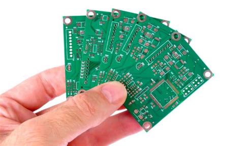
Introduction to PCB
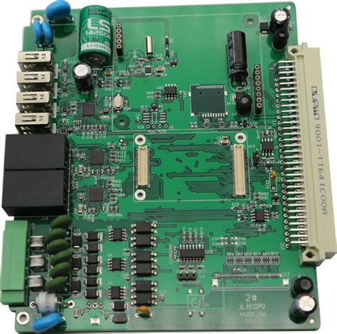
A Printed Circuit Board (PCB) is a fundamental component in modern electronic devices. It is a flat board made of insulating materials, such as fiberglass or composite epoxy, with conductive pathways etched or printed onto its surface. These pathways, also known as traces, connect various electronic components, such as resistors, capacitors, and integrated circuits, to form a complete electrical circuit.
PCBs have revolutionized the electronics industry by providing a reliable, compact, and cost-effective means of assembling electronic circuits. They are used in a wide range of applications, from simple consumer electronics to complex aerospace and military systems.
Key components of a PCB
- Substrate: The insulating base material, typically made of fiberglass or composite epoxy.
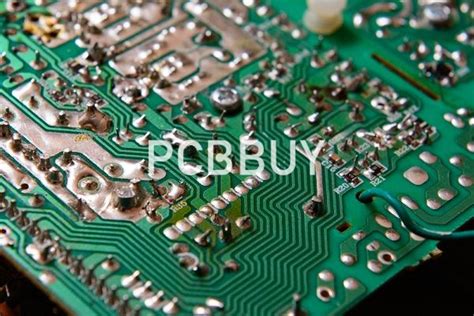
- Copper layers: Thin sheets of copper laminated onto the substrate, forming the conductive pathways.
- Solder mask: A protective coating applied over the copper layers, leaving only the exposed areas for soldering.
- Silkscreen: A printed layer that adds text, logos, and component identifiers to the PCB surface.
PCB Design and manufacturing process
PCB design workflow
- Schematic design: Creating a schematic diagram that represents the electrical connections between components.
- PCB layout: Translating the schematic into a physical layout, determining the placement of components and routing of traces.
- Design rule check (DRC): Verifying that the PCB layout adheres to the manufacturing constraints and design guidelines.
- Gerber file generation: Exporting the PCB layout as a set of Gerber files, which are used by the manufacturer to produce the board.
PCB Manufacturing Steps
- Copper clad lamination: Bonding copper foil to the substrate material using heat and pressure.
- Drilling: Creating holes for through-hole components and vias using CNC machines.
- Patterning: Transferring the PCB layout onto the copper layers using photolithography or silk-screening techniques.
- Etching: Removing unwanted copper from the board, leaving only the desired traces.
- Solder mask application: Applying a protective coating over the copper traces, exposing only the areas intended for soldering.
- Surface finish: Applying a final coating, such as HASL, ENIG, or OSP, to protect the exposed copper and facilitate soldering.
- Silkscreen printing: Adding text, logos, and component identifiers to the PCB surface.
- Electrical testing: Verifying the functionality and continuity of the PCB before assembly.
PCB classification and types
PCBs can be classified based on various factors, such as the number of layers, the type of material used, and the manufacturing process employed.
Number of layers
- Single-sided PCB: Has conductive traces on only one side of the substrate.
- Double-sided PCB: Has conductive traces on both sides of the substrate, with through-hole connections.
- Multi-layer PCB: Has three or more conductive layers, with insulating layers separating them.
Material types
- FR-4: The most common PCB substrate material, made of fiberglass reinforced with epoxy resin.
- CEM-1: A less expensive alternative to FR-4, made of a composite epoxy material with a cellulose paper core.
- Polyimide: A high-temperature, flexible substrate material used in applications requiring increased durability and thermal stability.
- Aluminum: A metal-core PCB substrate that provides excellent thermal conductivity for heat dissipation.
Manufacturing processes
- Through-hole technology (THT): Components are inserted into drilled holes and soldered on the opposite side of the board.
- Surface mount technology (SMT): Components are mounted directly onto the surface of the PCB, allowing for smaller footprints and higher component density.
- Mixed technology: A combination of THT and SMT components on the same PCB.

PCB design considerations and best practices
Designing a PCB involves various considerations to ensure optimal performance, manufacturability, and reliability. Some key aspects to consider include:
Signal integrity
- Impedance matching: Ensuring that the characteristic impedance of the traces matches the impedance of the connected components to minimize signal reflections and distortions.
- Crosstalk reduction: Minimizing the coupling of signals between adjacent traces by maintaining adequate spacing and using ground planes.
- Electromagnetic interference (EMI) mitigation: Implementing shielding, grounding, and filtering techniques to reduce EMI susceptibility and emissions.
Thermal management
- Heat dissipation: Selecting appropriate substrate materials and incorporating thermal vias and heatsinks to dissipate heat generated by components effectively.
- Component placement: Arranging components in a way that promotes even heat distribution and prevents localized hot spots.
Manufacturability
- Design for manufacturing (DFM): Adhering to the manufacturer’s design rules and guidelines to ensure that the PCB can be reliably and cost-effectively produced.
- Panelization: Grouping multiple PCB designs onto a single panel to optimize material usage and minimize manufacturing costs.
Assembly and testing
- Design for assembly (DFA): Considering the placement and orientation of components to facilitate automated assembly processes.
- Testability: Incorporating test points and boundary scan features to enable efficient testing and debugging of the assembled PCB.
PCB industry trends and future developments
The PCB industry is constantly evolving, driven by advancements in technology, changing market demands, and the need for more sophisticated and compact electronic devices. Some notable trends and future developments include:
Miniaturization
- Smaller component packages: The adoption of smaller surface-mount components, such as chip-scale packages (CSP) and ball grid arrays (BGA), enables higher component density and reduced PCB size.
- High-density interconnect (HDI): The use of micro-vias, blind and buried vias, and fine-pitch traces allows for more complex and compact PCB designs.
Advanced materials
- High-frequency laminates: The development of low-loss, high-frequency substrate materials enables the design of PCBs for high-speed digital and RF applications.
- Embedded components: Integrating passive components, such as resistors and capacitors, directly into the PCB substrate reduces the overall size and improves performance.
Additive manufacturing
- 3D printing: The use of 3D printing techniques, such as inkjet printing and stereolithography, enables the fabrication of complex, three-dimensional PCB Structures and rapid prototyping.
- Printed electronics: The development of conductive inks and flexible substrates allows for the printing of electronic circuits on various materials, expanding the range of PCB Applications.
Environmental sustainability
- Lead-free materials: The transition to lead-free solder alloys and finishes, driven by environmental regulations such as the Restriction of Hazardous Substances (RoHS) directive.
- Recyclability: The development of recyclable PCB substrate materials and the implementation of end-of-life recycling processes to minimize electronic waste.
Conclusion
The PCB is a critical component in modern electronics, providing a reliable and efficient means of interconnecting electronic components. Its design and manufacturing process involves various considerations, from material selection and layout optimization to signal integrity and thermal management.
As technology advances and market demands evolve, the PCB industry continues to innovate, adopting new materials, manufacturing techniques, and design methodologies. Miniaturization, advanced materials, additive manufacturing, and environmental sustainability are among the key trends shaping the future of PCB design and manufacturing.
Frequently Asked Questions (FAQ)
-
Q: What is the difference between a single-sided and double-sided PCB?
A: A single-sided PCB has conductive traces on only one side of the substrate, while a double-sided PCB has conductive traces on both sides, with through-hole connections between the layers. -
Q: What is the purpose of a solder mask on a PCB?
A: A solder mask is a protective coating applied over the copper traces on a PCB, leaving only the areas intended for soldering exposed. It prevents short circuits, protects the traces from environmental damage, and provides electrical insulation. -
Q: What is the difference between through-hole technology (THT) and surface mount technology (SMT)?
A: In THT, components are inserted into drilled holes and soldered on the opposite side of the board. In SMT, components are mounted directly onto the surface of the PCB, allowing for smaller footprints and higher component density. -
Q: What is the role of a PCB in thermal management?
A: A PCB plays a crucial role in thermal management by providing a means to dissipate heat generated by electronic components. This is achieved through the selection of appropriate substrate materials, the use of thermal vias and heatsinks, and the strategic placement of components to promote even heat distribution. -
Q: What are some of the key trends in the PCB industry?
A: Some of the key trends in the PCB industry include miniaturization, the adoption of advanced materials, the use of additive manufacturing techniques, and a focus on environmental sustainability through the use of lead-free materials and recyclable substrates.
Leave a Reply