What is a Printed Circuit board (PCB)?
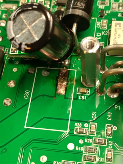
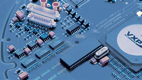
A Printed Circuit Board (PCB) is a thin board made of fiberglass or composite material that is used to mechanically support and electrically connect electronic components. PCBs are essential in the manufacturing of electronic devices, as they provide a reliable and efficient means of connecting components in a compact and organized manner.
How are PCBs manufactured?
The manufacturing process of PCBs involves several steps:
-
Designing the PCB layout: The first step is to design the PCB layout using specialized software. The layout includes the placement of components, the routing of conductive tracks, and the creation of any necessary vias or holes.
-
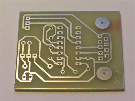
Printing the circuit pattern: Once the design is finalized, the circuit pattern is printed onto a copper-clad board using a photoresist process. The exposed areas of the copper are etched away, leaving only the desired conductive tracks.
-
Drilling holes: Holes are drilled into the board to accommodate through-hole components or to create vias that connect different layers of the PCB.
-
Applying solder mask and silkscreen: A solder mask is applied to the board to protect the copper tracks from oxidation and to prevent solder bridges during the assembly process. A silkscreen layer is also added to label components and provide other visual information.
-
Assembling components: Finally, the electronic components are soldered onto the PCB using either through-hole or surface-mount technology.
Types of PCBs
There are several types of PCBs, each with its own unique characteristics and applications:
-
Single-layer PCBs: These are the most basic type of PCBs, with components and conductive tracks on only one side of the board. They are commonly used in simple electronic devices.
-
Double-layer PCBs: These PCBs have components and conductive tracks on both sides of the board, allowing for more complex circuits and higher component density.
-
Multi-layer PCBs: These PCBs consist of three or more layers of conductive tracks, separated by insulating layers. They are used in high-density, complex electronic devices that require a large number of interconnections.
-
Flexible PCBs: These PCBs are made from flexible materials, such as polyimide, and can be bent or folded to fit into tight spaces or conform to specific shapes.
-
Rigid-Flex PCBs: These PCBs combine rigid and flexible sections, allowing for the benefits of both types of boards in a single design.
Applications of PCBs
PCBs are used in a wide range of electronic devices, from simple consumer gadgets to complex industrial equipment. Some common applications include:
-
Consumer electronics: PCBs are found in smartphones, tablets, laptops, televisions, and many other consumer electronic devices.
-
Automotive electronics: Modern vehicles rely heavily on electronic systems, such as engine control units, infotainment systems, and advanced driver assistance systems (ADAS), all of which utilize PCBs.
-
Medical devices: PCBs are essential in medical equipment, such as patient monitors, imaging systems, and implantable devices.
-
Industrial equipment: PCBs are used in various industrial applications, including process control systems, automation equipment, and power electronics.
-
Aerospace and defense: High-reliability PCBs are used in aerospace and defense applications, where failure is not an option.
Advantages of using PCBs
Using PCBs in electronic devices offers several advantages:
-
Compact size: PCBs allow for the dense packaging of electronic components, resulting in smaller and more compact devices.
-
Reliability: PCBs provide a stable and reliable means of connecting components, reducing the risk of loose connections or short circuits.
-
Reduced wiring: By etching conductive tracks directly onto the board, PCBs eliminate the need for complex wiring, making the assembly process more efficient and less error-prone.
-
Improved signal integrity: PCBs can be designed to minimize signal interference and crosstalk, ensuring the proper functioning of the electronic device.
-
Cost-effective: Mass production of PCBs is highly cost-effective, as the manufacturing process can be automated and optimized for high volumes.

Challenges in PCB design and manufacturing
Despite the many advantages of using PCBs, there are also some challenges that designers and manufacturers must address:
-
Signal integrity: As electronic devices become faster and more complex, maintaining signal integrity becomes increasingly difficult. Designers must carefully consider factors such as impedance matching, crosstalk, and electromagnetic interference (EMI) when creating PCB layouts.
-
Thermal management: High-powered electronic components generate significant amounts of heat, which must be dissipated to prevent damage to the device. PCBs must be designed with proper thermal management in mind, using techniques such as heat sinks, thermal vias, and active cooling.
-
Manufacturing limitations: PCB manufacturers have certain limitations in terms of minimum feature sizes, hole sizes, and spacing between components. Designers must work within these constraints to ensure that their boards can be manufactured reliably and cost-effectively.
-
Component availability: The global electronics supply chain can be volatile, with shortages and lead times for certain components fluctuating over time. PCB designers must be mindful of component availability and may need to make design adjustments to accommodate supply chain issues.
-
Environmental concerns: The manufacturing process for PCBs involves the use of chemicals and materials that can be harmful to the environment if not properly managed. Manufacturers must adhere to strict environmental regulations and implement proper waste management practices to minimize their ecological impact.
Future trends in PCB technology
As electronic devices continue to evolve, so too will PCB technology. Some of the future trends in PCB design and manufacturing include:
-
Miniaturization: The demand for smaller, more compact electronic devices will drive the development of ever-smaller PCBs with higher component densities.
-
High-speed design: As data rates continue to increase, PCBs will need to be designed to handle high-speed signals without compromising signal integrity.
-
Advanced materials: New materials, such as high-frequency laminates and low-loss dielectrics, will be developed to meet the demands of high-speed, high-frequency applications.
-
Embedded components: To further increase component density and reduce board size, some components may be embedded directly into the PCB substrate.
-
3D printing: Additive manufacturing techniques, such as 3D printing, may be used to create PCBs with complex geometries and unique features that are difficult or impossible to achieve with traditional manufacturing methods.
FAQ
-
Q: What is the difference between through-hole and surface-mount components?
A: Through-hole components have leads that are inserted into holes drilled in the PCB and soldered on the opposite side. Surface-mount components are soldered directly onto pads on the surface of the PCB, allowing for higher component density and smaller board sizes. -
Q: What is the purpose of a solder mask on a PCB?
A: A solder mask is a protective layer applied to the copper traces on a PCB. It prevents solder from bridging between adjacent traces during the assembly process and protects the copper from oxidation and contamination. -
Q: What is the difference between a rigid and a flexible PCB?
A: A rigid PCB is made from a solid, non-flexible material, such as fiberglass or epoxy. A flexible PCB is made from a flexible material, such as polyimide, and can be bent or folded to fit into tight spaces or conform to specific shapes. -
Q: What is the role of vias in a PCB?
A: Vias are small holes drilled through a PCB that allow electrical connections to be made between different layers of the board. They are used to route signals and power between components on different layers, allowing for more complex circuit designs in a compact space. -
Q: How are PCBs tested for quality and reliability?
A: PCBs undergo various tests to ensure quality and reliability, including visual inspections, automated optical inspections (AOI), X-ray inspections, and electrical tests such as continuity and insulation resistance tests. Additionally, boards may be subjected to environmental stress tests, such as thermal cycling and humidity exposure, to verify their durability under different operating conditions.
| Category | Examples |
|---|---|
| Consumer electronics | Smartphones, tablets, laptops, televisions |
| Automotive | Engine control units, infotainment systems, advanced driver assistance systems (ADAS) |
| Medical devices | Patient monitors, imaging systems, implantable devices |
| Industrial equipment | Process control systems, automation equipment, power electronics |
| Aerospace & defense | Avionics, communication systems, radar systems |
In conclusion, PCBs are an essential component in modern electronics, providing a reliable and efficient means of connecting electronic components in a compact and organized manner. As electronic devices continue to advance, PCB technology will evolve to meet the demands of increasingly complex and high-performance applications, while also addressing challenges related to signal integrity, thermal management, and environmental sustainability.
Leave a Reply