Introduction to PCBs
A Printed Circuit Board, commonly known as a PCB, is the backbone of nearly all electronic devices we use today. From smartphones and laptops to medical equipment and aerospace technology, PCBs play a crucial role in connecting and supporting various electronic components. In this beginner’s guide, we’ll dive into the basics of PCBs, their types, manufacturing process, and applications.
What is a PCB?
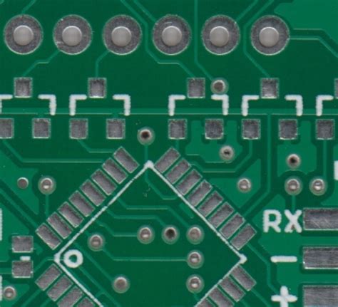
A PCB is a flat board made of insulating materials, such as fiberglass or composite epoxy, with conductive pathways etched or printed onto its surface. These pathways, called traces, connect various electronic components, such as resistors, capacitors, and integrated circuits (ICs), to create a functional electronic circuit.
PCBs offer several advantages over traditional wire-wrap or point-to-point construction:
- Compact size
- Improved reliability
- Reduced electronic noise
- Easier mass production
- Lower manufacturing costs

Types of PCBs
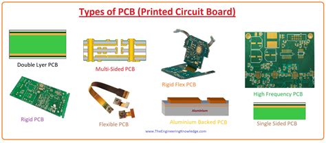
PCBs come in various types, each with its own unique features and applications. The most common types include:
1. Single-layer PCBs
Single-layer PCBs have conductive traces on only one side of the board. They are the simplest and most cost-effective type of PCB, suitable for basic electronic projects and low-density designs.
2. Double-layer PCBs
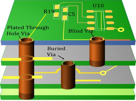
Double-layer PCBs have conductive traces on both sides of the board, allowing for more complex circuit designs and higher component density compared to single-layer PCBs. The two layers are connected using through-hole vias.
3. Multi-layer PCBs
Multi-layer PCBs consist of three or more conductive layers separated by insulating materials. They offer the highest component density and are used in complex electronic devices, such as smartphones, computers, and medical equipment.
4. Flexible PCBs
Flexible PCBs are made using flexible substrate materials, such as polyimide or PEEK, allowing the board to bend and conform to various shapes. They are commonly used in wearable electronics, automobiles, and aerospace applications.
5. Rigid-Flex PCBs
Rigid-Flex PCBs combine the benefits of both rigid and flexible PCBs, featuring rigid sections for mounting components and flexible sections for connecting multiple rigid boards or conforming to unique shapes.

PCB Manufacturing Process
The PCB manufacturing process involves several steps, each requiring precision and attention to detail. The main steps include:
-
PCB design: The circuit schematic is created using Electronic Design Automation (EDA) software, which generates the necessary files for manufacturing, such as Gerber and drill files.
-
PCB fabrication: The fabrication process begins with the creation of a substrate, typically made of fiberglass or composite epoxy. Copper foil is then laminated onto the substrate, and the conductive patterns are etched using photolithography and chemical etching techniques.
-
Drilling: Holes are drilled into the PCB to accommodate through-hole components and vias.
-
Plating: The holes are plated with conductive materials, such as copper or gold, to ensure proper electrical connectivity.
-
Solder Mask Application: A protective solder mask is applied to the PCB surface, leaving only the exposed pads and connectors for soldering.
-
Silkscreen Printing: Text, logos, and component identifiers are printed onto the PCB surface using silkscreen printing for easy identification and assembly.
-
Surface Finish: A surface finish, such as HASL (Hot Air Solder Leveling) or ENIG (Electroless Nickel Immersion Gold), is applied to the exposed pads to prevent oxidation and improve solderability.
-
Electrical Testing: The PCB undergoes various electrical tests to ensure proper functionality and adherence to design specifications.
-
Component Assembly: Electronic components are soldered onto the PCB, either through automated processes like SMT (Surface Mount Technology) or manual through-hole soldering.

PCB Design Considerations
When designing a PCB, several factors must be considered to ensure optimal performance and manufacturability:
-
Component Placement: Components should be placed logically, minimizing the distance between connected components and reducing the overall PCB size.
-
Trace Width and Spacing: The width and spacing of the conductive traces should be adequate to handle the required current and voltage while minimizing crosstalk and electromagnetic interference (EMI).
-
Power and Ground Planes: Dedicated power and ground planes help distribute power evenly across the PCB and reduce noise.
-
Signal Integrity: High-speed signals require careful routing and impedance control to maintain signal integrity and minimize reflections and crosstalk.
-
Thermal Management: Proper thermal management, such as the use of heatsinks and thermal vias, is crucial for dissipating heat generated by power-hungry components.
-
Manufacturing Constraints: PCB design must adhere to the manufacturing capabilities of the chosen fabrication house, including minimum trace width, hole size, and clearance.
PCB Testing and Inspection
To ensure the quality and reliability of PCBs, various testing and inspection methods are employed:
-
Visual Inspection: PCBs are visually inspected for defects, such as incorrect component placement, solder bridges, or damaged traces.
-
Automated Optical Inspection (AOI): AOI systems use high-resolution cameras and image processing algorithms to detect surface-level defects.
-
X-ray Inspection: X-ray imaging is used to inspect hidden features, such as ball grid array (BGA) solder joints and internal traces.
-
In-Circuit Testing (ICT): ICT involves probing individual components and circuits to verify their functionality and adherence to design specifications.
-
Functional Testing: The PCB is tested as a complete system to ensure it performs its intended function under various operating conditions.
Applications of PCBs
PCBs find applications in nearly every electronic device and system. Some common applications include:
-
Consumer Electronics: Smartphones, laptops, tablets, televisions, and home appliances.
-
Automotive: Engine control units, infotainment systems, and advanced driver assistance systems (ADAS).
-
Medical Devices: Diagnostic equipment, patient monitoring systems, and implantable devices.
-
Industrial Automation: Programmable logic controllers (PLCs), sensors, and motor drives.
-
Aerospace and Defense: Avionics, communication systems, and military equipment.
-
Internet of Things (IoT): Smart home devices, wearables, and sensor networks.
Frequently Asked Questions (FAQ)
1. What is the difference between a PCB and a breadboard?
A breadboard is a prototyping tool used for temporary circuit construction and testing, while a PCB is a permanent, reliable, and compact solution for electronic circuits.
2. Can I design my own PCB?
Yes, with the help of EDA software and basic electronics knowledge, you can design your own PCB. However, complex designs may require professional expertise.
3. How long does it take to manufacture a PCB?
The manufacturing time depends on the complexity of the design and the fabrication house’s capacity. Simple PCBs can be manufactured within a few days, while complex designs may take several weeks.
4. What is the cost of manufacturing a PCB?
The cost of manufacturing a PCB depends on various factors, such as the board size, layer count, component density, and order quantity. Small, simple PCBs can cost a few dollars, while complex, high-density PCBs can cost hundreds or even thousands of dollars.
5. How do I choose the right PCB manufacturer?
When choosing a PCB manufacturer, consider factors such as their experience, manufacturing capabilities, quality control processes, turnaround time, and customer support. Read reviews and request quotes from multiple manufacturers before making a decision.
Conclusion
PCBs are the foundation of modern electronics, enabling the creation of compact, reliable, and cost-effective electronic devices. By understanding the basics of PCBs, their types, manufacturing process, and design considerations, you can better appreciate the complexities and challenges involved in bringing electronic products to life. As technology advances, PCBs will continue to play a crucial role in shaping the future of electronics.

Leave a Reply