Introduction to PCBs
A Printed Circuit Board (PCB) is a fundamental component in modern electronics. It is a thin board made of insulating materials, such as fiberglass or composite epoxy, with conductive copper traces printed onto its surface. These traces connect various electronic components, such as resistors, capacitors, and integrated circuits, to create a functional electronic device. PCBs have revolutionized the electronics industry by providing a reliable, compact, and cost-effective means of assembling electronic circuits.
The History of PCBs
The concept of PCBs dates back to the early 20th century when inventors began exploring ways to simplify the wiring of electronic devices. In 1925, Charles Ducas filed a patent for a method of creating an electrical path directly on an insulated surface. However, it wasn’t until the 1940s that PCBs began to gain widespread use, primarily in military applications during World War II.
In the 1950s and 1960s, PCB manufacturing techniques improved, making them more accessible for commercial use. The introduction of through-hole technology, where components were inserted into drilled holes and soldered onto the board, became the standard method of PCB assembly.
As electronics became more complex and compact, surface-mount technology (SMT) emerged in the 1980s. SMT allows for smaller components to be placed directly onto the surface of the PCB, enabling the creation of high-density designs.
PCB Functionality
Basic Structure
A PCB consists of several layers, each serving a specific purpose:
-
Substrate: The base material, typically made of fiberglass or composite epoxy, provides insulation and mechanical support for the copper traces and components.
-
Copper Layers: Thin sheets of copper are laminated onto the substrate. These layers are etched to create conductive traces that connect the components. A PCB can have one or multiple copper layers, depending on the complexity of the design.
-
Solder Mask: A protective coating applied over the copper traces, leaving only the areas intended for soldering exposed. The solder mask helps prevent short circuits and provides insulation between adjacent traces.
-
Silkscreen: A printed layer that adds text, logos, and component identifiers to the PCB, making it easier to assemble and troubleshoot.
Circuit Design and Layout
Creating a functional PCB involves several steps:
-
Schematic Design: Engineers use electronic design automation (EDA) software to create a schematic diagram of the circuit. This diagram shows the interconnections between components and defines the electrical functionality of the device.
-
Component Selection: Based on the schematic, engineers choose the appropriate components for the PCB, considering factors such as power requirements, size constraints, and cost.
-
PCB Layout: Using EDA software, designers create a physical layout of the PCB, arranging the components and routing the copper traces to ensure proper connectivity and minimize interference.
-
Design Rule Check (DRC): Before manufacturing, the PCB layout undergoes a DRC to verify that it meets the specified design rules, such as minimum trace widths and clearances between components.
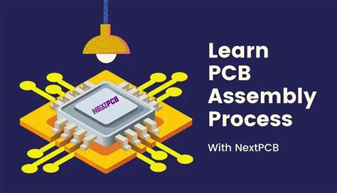
Manufacturing Process
Once the PCB design is finalized, it enters the manufacturing process:
-
PCB Fabrication: The designed layout is used to create a photomask, which is then used to transfer the circuit pattern onto the copper-clad substrate through a photolithographic process. The unwanted copper is etched away, leaving only the desired traces.
-
Drilling: Holes are drilled into the PCB to accommodate through-hole components and provide interconnections between layers.
-
Plating: The holes are plated with copper to create electrical connections between layers.
-
Solder Mask and Silkscreen Application: The solder mask and silkscreen layers are applied to the PCB.
-
Surface Finish: A protective finish, such as lead-free Hot Air Solder Leveling (HASL) or Electroless Nickel Immersion Gold (ENIG), is applied to the exposed copper areas to prevent oxidation and improve solderability.
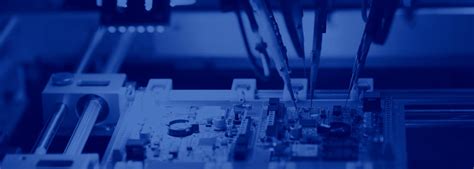
PCB Assembly
After the PCB is manufactured, it undergoes the assembly process:
-
Solder Paste Application: For surface-mount components, solder paste is applied to the pads on the PCB using a stencil or screen printing process.
-
Component Placement: Surface-mount components are placed onto the solder paste using pick-and-place machines, while through-hole components are inserted manually or by machine into the drilled holes.
-
Soldering: The PCB is heated in a reflow oven, causing the solder paste to melt and form electrical connections between the components and the copper traces. Through-hole components are soldered using wave soldering or manual soldering techniques.
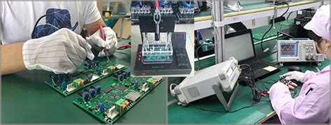
-
Inspection and Testing: The assembled PCB undergoes visual inspection and automated optical inspection (AOI) to detect any defects or misaligned components. Functional testing is also performed to ensure that the PCB operates as intended.

Types of PCBs
PCBs can be categorized based on the number of copper layers and their manufacturing process:
Single-Layer PCBs
Single-layer PCBs have copper traces on only one side of the substrate. They are the simplest and most cost-effective type of PCB, suitable for basic electronic devices with low component density.
Double-Layer PCBs
Double-layer PCBs have copper traces on both sides of the substrate, allowing for more complex routing and higher component density compared to single-layer PCBs. The two layers are connected using through-hole vias.
Multi-Layer PCBs
Multi-layer PCBs consist of three or more copper layers, with insulating layers separating them. These PCBs offer the highest component density and are used in complex electronic devices, such as smartphones, computers, and medical equipment. The layers are interconnected using through-hole vias and blind or buried vias, which are drilled and plated to connect specific layers without going through the entire board.
Flexible PCBs
Flexible PCBs are made using a thin, flexible substrate, such as polyimide or polyester. They can bend and conform to various shapes, making them ideal for applications where space is limited or the device requires movement, such as in wearable electronics or automotive systems.
Rigid-Flex PCBs
Rigid-flex PCBs combine the benefits of both rigid and flexible PCBs. They consist of rigid PCB sections connected by flexible PCB sections, allowing for three-dimensional packaging and improved reliability in applications with high vibration or mechanical stress.
PCB Functionality in Various Applications
PCBs play a crucial role in a wide range of electronic applications, from consumer gadgets to industrial equipment and aerospace systems. Here are some examples:
Consumer Electronics
-
Smartphones and Tablets: PCBs in these devices house components like processors, memory, sensors, and connectivity modules, enabling the compact and feature-rich designs we rely on daily.
-
Wearable Devices: Smartwatches, fitness trackers, and hearables use flexible or rigid-flex PCBs to achieve small form factors and withstand the stresses of daily wear.
-
Home Appliances: PCBs control and power various home appliances, such as refrigerators, washing machines, and air conditioners, enabling smart features and energy efficiency.
Industrial Applications
-
Automation and Control Systems: PCBs are used in programmable logic controllers (PLCs), human-machine interfaces (HMIs), and sensors, facilitating the control and monitoring of industrial processes.
-
Power Electronics: High-power PCBs with thick copper traces and robust heat dissipation are used in motor drives, inverters, and power supplies for industrial machinery.
-
Medical Devices: PCBs are essential in medical equipment like patient monitors, imaging systems, and diagnostic tools, ensuring reliable operation and patient safety.
Automotive Applications
-
Engine Control Units (ECUs): PCBs in ECUs manage various aspects of a vehicle’s performance, such as fuel injection, ignition timing, and emissions control.
-
Infotainment Systems: PCBs enable the functionality of in-car entertainment, navigation, and communication systems, providing drivers and passengers with a seamless user experience.
-
Advanced Driver Assistance Systems (ADAS): PCBs in ADAS components, like cameras, radar, and lidars, process and analyze data to enable features such as lane departure warnings, adaptive cruise control, and automatic emergency braking.
Aerospace and Defense
-
Avionics: PCBs in aircraft control systems, navigation equipment, and communication devices ensure reliable operation in harsh environments and meet stringent safety requirements.
-
Satellites: High-reliability PCBs with radiation-hardened components are used in satellite systems to withstand the challenges of space, such as extreme temperatures and cosmic radiation.
-
Military Equipment: PCBs in military applications, like tactical communication devices, guidance systems, and surveillance equipment, are designed to be rugged, secure, and operate in hostile environments.
PCB Design Considerations
Designing a functional and reliable PCB requires careful consideration of various factors:
Signal Integrity
As electronic devices become faster and more complex, maintaining signal integrity is crucial. Designers must consider factors such as impedance matching, crosstalk, and electromagnetic interference (EMI) when routing traces and placing components on the PCB.
Power Integrity
Ensuring a stable and clean power supply is essential for the proper functioning of electronic components. PCB designers must carefully plan the power distribution network, considering factors such as voltage drops, current requirements, and decoupling capacitor placement.
Thermal Management
Heat generated by electronic components can affect the performance and reliability of the PCB. Designers must incorporate thermal management techniques, such as using heatsinks, thermal vias, and proper component placement, to dissipate heat effectively.
Manufacturing Constraints
PCB designers must adhere to manufacturing constraints, such as minimum trace widths, clearances, and drill sizes, to ensure that the PCB can be manufactured reliably and cost-effectively.
Testing and Debugging
Designing the PCB with testing and debugging in mind can significantly simplify the development process. Incorporating test points, debug connectors, and clear silkscreen markings can help engineers quickly identify and resolve issues during prototyping and production.
Future Trends in PCB Technology
As electronic devices continue to evolve, PCB technology must adapt to meet new challenges and demands:
High-Speed PCBs
With the increasing data rates in communication systems and high-performance computing, PCBs must support higher signal speeds. Advanced materials, such as low-loss substrates and high-speed laminates, along with sophisticated design techniques, like differential signaling and controlled impedance routing, will be essential for high-speed PCBs.
Miniaturization
The trend towards smaller, more compact electronic devices will drive the need for higher-density PCBs. Advanced packaging technologies, such as chip-on-board (COB) and system-in-package (SiP), will enable the integration of more functionality into smaller form factors.
Additive Manufacturing
Additive manufacturing techniques, like 3D printing, are emerging as a potential alternative to traditional PCB manufacturing methods. These techniques can enable the creation of complex, three-dimensional PCB Structures and reduce waste material during production.
Eco-Friendly Materials
As environmental concerns grow, there will be an increasing demand for eco-friendly PCB materials and manufacturing processes. Bio-based substrates, halogen-free laminates, and lead-free solders will become more prevalent in the industry.
Embedded Components
Embedding components, such as resistors, capacitors, and even active devices, within the PCB substrate can save space, improve signal integrity, and enhance reliability. As this technology matures, it will enable the creation of more compact and efficient electronic devices.
Frequently Asked Questions (FAQ)
-
What is the difference between a PCB and a breadboard?
A breadboard is a prototyping tool that allows for the temporary connection of electronic components without soldering. It is useful for quickly testing and modifying circuit designs. In contrast, a PCB is a permanent, manufactured board with copper traces that provide a reliable and compact solution for electronic circuits. -
Can PCBs be repaired?
Yes, PCBs can be repaired, depending on the extent of the damage and the complexity of the board. Common repair techniques include soldering, trace repair, and component replacement. However, for complex, multi-layer PCBs or extensive damage, repair may not be feasible, and replacement may be necessary. -
What is the difference between through-hole and surface-mount components?
Through-hole components have long leads that are inserted into drilled holes on the PCB and soldered on the opposite side. They are generally larger and easier to work with manually. Surface-mount components are smaller and have short leads or pads that are soldered directly onto the surface of the PCB. Surface-mount components enable higher-density designs and automated assembly processes. -
How do I choose the right PCB material for my application?
Choosing the right PCB material depends on factors such as the operating environment, signal speed, and cost. Common PCB materials include FR-4, which is a standard fiberglass-reinforced epoxy laminate, and high-frequency laminates like Rogers or Isola for high-speed applications. Flexible materials like polyimide are used for flexible PCBs. Consult with a PCB manufacturer or materials expert to select the most appropriate material for your specific application. -
What is the typical turnaround time for PCB fabrication?
The turnaround time for PCB fabrication varies depending on the complexity of the design, the chosen manufacturer, and the required quantity. For standard PCBs, turnaround times can range from a few days to a couple of weeks. Expedited services are often available for an additional cost. It is essential to communicate your timeline requirements with the PCB manufacturer and plan accordingly.
Conclusion
PCBs are the backbone of modern electronics, enabling the creation of compact, reliable, and cost-effective devices across various industries. Understanding the functionality, design considerations, and manufacturing processes of PCBs is crucial for engineers, designers, and anyone involved in the development of electronic products.
As technology continues to advance, PCBs will play an increasingly important role in shaping the future of electronics. By staying informed about the latest trends and techniques in PCB design and manufacturing, we can create innovative solutions that push the boundaries of what is possible in the world of electronics.
Leave a Reply