Understanding PCB DFM and Its Importance
PCB DFM (Design for Manufacturability) is a crucial aspect of the printed circuit board design process that ensures the manufacturability and reliability of the final product. By considering DFM guidelines and best practices during the design phase, engineers can minimize potential issues, reduce manufacturing costs, and improve the overall quality of the PCB.
What is PCB DFM?
PCB DFM is a set of design principles and guidelines that aim to optimize the PCB design for the manufacturing process. It takes into account various factors such as component placement, trace routing, pad sizes, and clearances to ensure that the PCB can be efficiently and reliably manufactured.
Why is PCB DFM Important?
Implementing DFM principles in your PCB design offers several benefits:
- Reduced manufacturing costs
- Improved PCB quality and reliability
- Faster time-to-market
- Fewer design iterations and rework
- Enhanced collaboration between design and manufacturing teams
Common PCB DFM Errors and How to Avoid Them
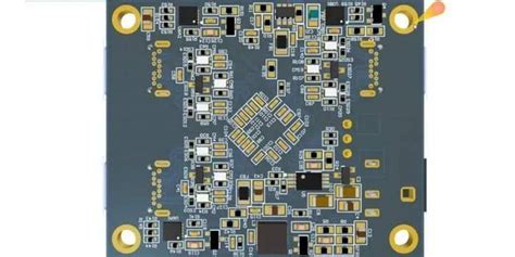
1. Incorrect Component Placement
One of the most common DFM errors is improper component placement. This can lead to manufacturing difficulties, signal integrity issues, and thermal management problems.
To avoid this error:
- Follow the manufacturer’s recommended placement guidelines
- Consider component orientation and spacing
- Place components in a logical and organized manner
- Use automated placement tools to optimize component placement
2. Insufficient Clearances
Insufficient clearances between components, traces, and other PCB elements can cause short circuits, manufacturing defects, and reliability issues.
To prevent this error:
- Adhere to the minimum clearance requirements specified by the PCB manufacturer
- Use design rule checks (DRC) to verify clearances
- Consider the manufacturing tolerances and adjust clearances accordingly
| Clearance Type | Minimum Distance |
|---|---|
| Trace to Trace | 0.15 mm |
| Pad to Pad | 0.20 mm |
| Component to Component | 0.50 mm |
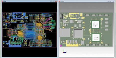
3. Incorrect Trace Width and Spacing
Using incorrect trace widths and spacing can lead to signal integrity issues, EMI problems, and manufacturing difficulties.
To avoid this error:
- Calculate the appropriate trace width based on the current carrying requirements
- Maintain consistent trace width and spacing throughout the design
- Follow the PCB manufacturer’s guidelines for minimum trace width and spacing
4. Inadequate Via Design
Vias are essential for connecting different layers of the PCB, but improper via design can cause manufacturing issues and affect signal integrity.
To prevent this error:
- Use an appropriate via size based on the PCB Thickness and layer count
- Maintain sufficient spacing between vias and other components
- Avoid placing vias under components unless necessary
- Use via stitching to improve thermal management and EMI shielding
5. Incorrect Solder Mask and Silkscreen
Solder mask and silkscreen errors can lead to assembly issues and make it difficult to identify components and their orientations.
To avoid this error:
- Ensure adequate solder mask expansion around pads and vias
- Provide clear and legible silkscreen labels for components
- Follow the manufacturer’s guidelines for solder mask and silkscreen design
Best Practices for PCB DFM
- Collaborate closely with the PCB manufacturer throughout the design process
- Use a checklist to ensure all DFM guidelines are followed
- Perform thorough design reviews and simulations to catch potential issues early
- Keep up-to-date with the latest DFM standards and guidelines
- Continuously monitor and improve the DFM process based on feedback and lessons learned

Frequently Asked Questions (FAQ)
1. What is the difference between PCB DFM and DFA?
PCB DFM (Design for Manufacturability) focuses on optimizing the PCB design for the manufacturing process, while DFA (Design for Assembly) concentrates on making the PCB easier to assemble. Both DFM and DFA are essential for creating a successful PCB design.
2. How can I ensure my PCB design meets DFM requirements?
To ensure your PCB design meets DFM requirements, follow these steps:
- Familiarize yourself with the PCB manufacturer’s DFM guidelines
- Use PCB design software that includes DFM checks and rules
- Collaborate with the PCB manufacturer and seek their feedback on your design
- Perform thorough design reviews and simulations to identify potential issues
3. What are the consequences of not following PCB DFM guidelines?
Not following PCB DFM guidelines can lead to various problems, such as:
- Manufacturing delays and increased costs
- Reduced PCB quality and reliability
- Increased risk of design iterations and rework
- Strained relationships between design and manufacturing teams
4. Can I use automated tools to help with PCB DFM?
Yes, there are several automated tools available to assist with PCB DFM, including:
- PCB design software with built-in DFM checks and rules
- Standalone DFM analysis tools that can identify potential issues
- Automated component placement and routing tools that optimize the design for manufacturability
5. How can I stay up-to-date with the latest PCB DFM standards and guidelines?
To stay up-to-date with the latest PCB DFM standards and guidelines, consider the following:
- Regularly engage with your PCB manufacturer and seek their expertise
- Attend industry conferences and webinars focused on PCB design and manufacturing
- Participate in online forums and communities dedicated to PCB design
- Read industry publications and blogs that cover PCB DFM topics
By understanding and implementing PCB DFM principles, engineers can create more manufacturable and reliable PCB designs, ultimately leading to faster time-to-market, lower costs, and improved product quality.
Leave a Reply