Introduction to PCB Transmission Lines
Printed Circuit Boards (PCBs) are the backbone of modern electronic devices, connecting various components and enabling signal transmission. As the demand for high-speed and high-frequency applications grows, the importance of understanding and optimizing PCB transmission lines becomes increasingly critical. This article will delve into the world of PCB Transmission line calculators, exploring their significance, types, and usage in PCB design.
What are PCB Transmission Lines?
PCB transmission lines are the copper traces on a PCB that carry electrical signals between components. These lines are designed to maintain signal integrity and minimize losses, ensuring reliable communication within the circuit. At high frequencies, the behavior of these transmission lines becomes more complex, requiring careful consideration of factors such as impedance matching, signal reflection, and crosstalk.
Why are PCB Transmission Line Calculators Important?
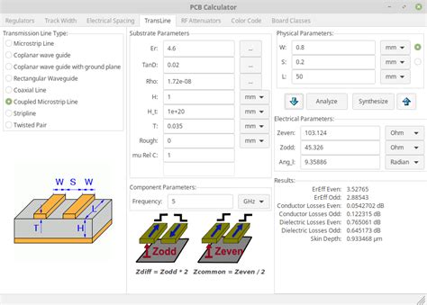
PCB transmission line calculators are essential tools for engineers and designers working on high-speed PCB designs. These calculators help determine the optimal geometry and materials for transmission lines, ensuring proper impedance matching and minimizing signal distortion. By using these calculators, designers can:
- Reduce signal integrity issues
- Minimize signal reflections and crosstalk
- Optimize PCB layout for high-speed applications
- Save time and resources in the design process
Types of PCB Transmission Lines
There are several types of PCB transmission lines, each with its own characteristics and applications. The most common types include:
Microstrip Lines
Microstrip lines are the most widely used type of PCB transmission line. They consist of a single conductor trace on the top layer of the PCB, with a ground plane on the bottom layer. The characteristics of microstrip lines are determined by the width of the trace, the thickness of the substrate, and the dielectric constant of the substrate material.
| Parameter | Description |
|---|---|
| W | Width of the trace |
| H | Thickness of the substrate |
| εr | Dielectric constant of the substrate |
Stripline
Striplines are another common type of PCB transmission line. They consist of a single conductor trace embedded between two ground planes, with the substrate material surrounding the trace. Striplines offer better shielding and reduced crosstalk compared to microstrip lines, but they require more layers in the PCB stack-up.
| Parameter | Description |
|---|---|
| W | Width of the trace |
| H | Distance between ground planes |
| εr | Dielectric constant of the substrate |
Coplanar Waveguide (CPW)
Coplanar waveguides are transmission lines that have the signal trace and ground planes on the same layer of the PCB. The signal trace is surrounded by two ground planes, which provide shielding and reduce crosstalk. CPWs are often used in high-frequency applications due to their low dispersion and ease of integration with surface-mount components.
| Parameter | Description |
|---|---|
| W | Width of the signal trace |
| G | Gap between signal trace and ground planes |
| εr | Dielectric constant of the substrate |

PCB Transmission Line Calculator Usage
Step 1: Determine the Required Impedance
The first step in using a PCB transmission line calculator is to determine the required characteristic impedance of the transmission line. This impedance is typically specified by the system requirements or the components connected to the transmission line. Common impedance values include 50Ω, 75Ω, and 100Ω.
Step 2: Select the Transmission Line Type
Choose the appropriate transmission line type based on your PCB design requirements. Consider factors such as the number of layers available, the desired shielding, and the ease of manufacturing.
Step 3: Input the PCB Parameters
Enter the relevant PCB parameters into the transmission line calculator. These parameters include the substrate material, its dielectric constant, the thickness of the substrate, and the desired trace width.
Step 4: Optimize the Transmission Line Geometry
Using the calculator, iterate on the transmission line geometry to achieve the desired characteristic impedance. Adjust the trace width, substrate thickness, or other parameters as needed.
Step 5: Verify the Results
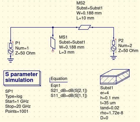
Once you have achieved the desired impedance, verify the results using simulation tools or by fabricating a test coupon. This step ensures that the calculated transmission line geometry performs as expected in the real world.

PCB Transmission Line Calculator Examples
To illustrate the usage of PCB transmission line calculators, let’s consider a few examples:
Example 1: Microstrip Line
- Desired Impedance: 50Ω
- Substrate Material: FR-4
- Dielectric Constant (εr): 4.3
- Substrate Thickness (H): 1.6 mm
Using a microstrip line calculator, we find that a trace width (W) of 2.8 mm results in a characteristic impedance of 50Ω.
Example 2: Stripline
- Desired Impedance: 75Ω
- Substrate Material: Rogers RO4350B
- Dielectric Constant (εr): 3.66
- Distance between Ground Planes (H): 1.524 mm
Using a stripline calculator, we find that a trace width (W) of 0.38 mm results in a characteristic impedance of 75Ω.

Frequently Asked Questions (FAQ)
-
Q: What is the difference between a microstrip line and a stripline?
A: A microstrip line has a single conductor trace on the top layer of the PCB, with a ground plane on the bottom layer. A stripline has a single conductor trace embedded between two ground planes, with the substrate material surrounding the trace. -
Q: How does the dielectric constant of the substrate material affect the transmission line?
A: The dielectric constant of the substrate material influences the speed of signal propagation and the characteristic impedance of the transmission line. A higher dielectric constant results in slower signal propagation and requires wider traces to achieve the same impedance. -
Q: What is the purpose of impedance matching in PCB transmission lines?
A: Impedance matching ensures that the characteristic impedance of the transmission line matches the impedance of the source and load. This minimizes signal reflections, which can cause signal integrity issues and degrade the performance of the system. -
Q: Can I use a PCB transmission line calculator for high-frequency applications?
A: Yes, PCB transmission line calculators are particularly useful for high-frequency applications, where the effects of impedance mismatch and signal reflections are more pronounced. However, it’s essential to verify the calculated results through simulations and measurements. -
Q: Are there any limitations to using PCB transmission line calculators?
A: PCB transmission line calculators provide a good starting point for designing transmission lines, but they have some limitations. They assume ideal conditions and may not account for all the factors that affect signal integrity, such as surface roughness, conductor losses, and dispersion. It’s always recommended to use simulation tools and perform measurements to validate the design.
Conclusion
PCB transmission line calculators are invaluable tools for engineers and designers working on high-speed PCB designs. By understanding the types of transmission lines and their characteristics, designers can use these calculators to optimize the geometry and materials of their PCB Traces. This optimization ensures proper impedance matching, minimizes signal integrity issues, and improves the overall performance of the electronic system.
When using PCB transmission line calculators, it’s essential to follow a systematic approach, starting with determining the required impedance and selecting the appropriate transmission line type. By inputting the relevant PCB parameters and iterating on the design, designers can achieve the desired characteristic impedance and verify the results through simulations and measurements.
As the demand for high-speed and high-frequency applications continues to grow, the role of PCB transmission line calculators in the design process will only become more critical. By leveraging these tools and understanding the principles behind transmission line design, engineers and designers can create robust, reliable, and high-performance electronic systems.

Leave a Reply