Introduction to PCB Manufacturing
Printed Circuit Boards (PCBs) are the backbone of modern electronics. They are used in almost every electronic device, from smartphones and computers to medical equipment and aerospace systems. PCBs provide a platform for electrical components to be mounted and connected, allowing for the creation of complex circuits in a compact and efficient manner.
Manufacturing small circuit boards, or PCBs, requires precision, expertise, and the right equipment. In this article, we will delve into the process of PCB manufacturing, covering everything from design and layout to fabrication and assembly.
The PCB Manufacturing Process
The PCB manufacturing process can be broken down into several key stages:
- Design and Layout
- Fabrication
- Assembly
- Testing and Quality Control
Let’s explore each of these stages in more detail.
Design and Layout
The first step in PCB manufacturing is designing the circuit board. This involves creating a schematic diagram that outlines the electrical connections between components, as well as a layout that determines the physical placement of those components on the board.
Schematic Design
The schematic design is a graphical representation of the electronic circuit. It uses standardized symbols to represent components like resistors, capacitors, and integrated circuits, and shows how they are connected electrically.
PCB Layout
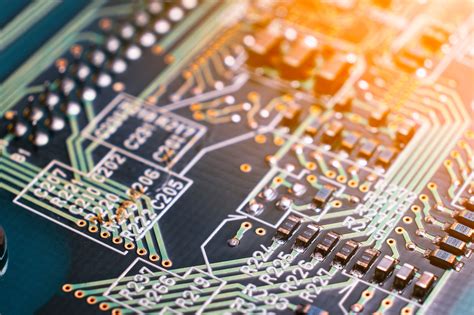
Once the schematic is complete, the next step is to create the PCB layout. This involves determining the physical location of each component on the board, as well as the routing of the copper traces that will connect them.
PCB layout is typically done using specialized software, such as Altium Designer, Eagle, or KiCad. These tools allow designers to create a virtual representation of the board, complete with component footprints and copper traces.
Some key considerations during PCB layout include:
- Component placement: Components should be placed in a logical manner that minimizes the length of copper traces and reduces the risk of interference.
- Trace width and spacing: The width and spacing of copper traces must be carefully calculated based on the current they will carry and the desired impedance of the circuit.
- Grounding and shielding: Proper grounding and shielding techniques are essential for reducing noise and ensuring the stability of the circuit.
Fabrication
Once the PCB design is complete, the next step is to fabricate the physical board. This involves several processes:
PCB Printing
The first step in PCB fabrication is to print the circuit pattern onto a copper-clad board. This is typically done using a photoresist process:
- The copper-clad board is coated with a light-sensitive photoresist material.
- The PCB layout is printed onto a transparency film, which is then placed on top of the photoresist-coated board.
- The board is exposed to UV light, which hardens the photoresist in the areas not covered by the transparency film.
- The unexposed photoresist is then removed using a chemical developer, leaving behind the circuit pattern.
Etching
After the circuit pattern has been printed, the next step is to remove the unwanted copper from the board. This is done using a chemical etching process:
- The board is immersed in an etchant solution, typically ferric chloride or ammonium persulfate.
- The etchant removes the copper that is not protected by the hardened photoresist, leaving behind the desired circuit pattern.
- The remaining photoresist is then stripped away, revealing the final copper traces.
Drilling
Most PCBs require holes to be drilled for component leads or vias (connections between layers). This is typically done using a computer-controlled drill machine.
PCB Lamination
For multi-layer PCBs, the individual layers must be laminated together under heat and pressure. This involves aligning the layers precisely and bonding them with a prepreg (pre-impregnated) material that acts as an insulating layer between the copper traces.
Surface Finishing
The final step in PCB fabrication is to apply a surface finish to protect the copper traces and improve solderability. Common surface finishes include:
- HASL (Hot Air Solder Leveling): A thin layer of solder is applied to the copper traces and then leveled using hot air.
- ENIG (Electroless Nickel Immersion Gold): A layer of nickel is deposited onto the copper, followed by a thin layer of gold.
- OSP (Organic Solderability Preservative): A thin, organic coating is applied to the copper to prevent oxidation.
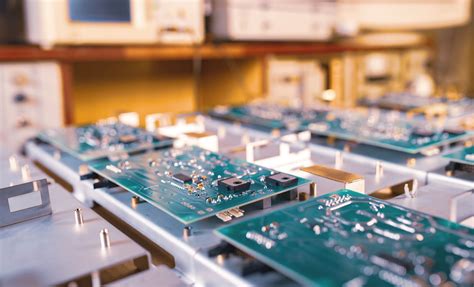
Assembly
With the fabricated PCB in hand, the next step is to assemble the components onto the board. This can be done manually for small quantities or prototypes, but for larger volumes, automated assembly processes are typically used.
SMT (Surface Mount Technology)
SMT is the most common method for assembling PCBs. It involves placing components directly onto the surface of the board and soldering them in place. The process typically involves:
- Solder paste application: A thin layer of solder paste is applied to the pads where components will be placed.
- Pick and place: An automated machine picks up components and places them onto the solder paste.
- Reflow soldering: The board is passed through a reflow oven, which melts the solder paste and bonds the components to the board.
THT (Through-Hole Technology)
THT involves inserting component leads through holes in the board and soldering them in place. This method is less common than SMT but is still used for certain types of components, such as connectors or large transformers.
Testing and Quality Control
The final step in PCB manufacturing is testing and quality control. This involves several processes to ensure that the board is functioning correctly and meets the required specifications.
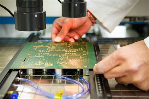
Automated Optical Inspection (AOI)
AOI uses cameras and computer vision algorithms to inspect the board for defects such as missing components, solder bridges, or incorrect component placement.
In-Circuit Testing (ICT)
ICT involves using a bed-of-nails fixture to make electrical contact with specific points on the board and test the functionality of individual components and circuits.
Functional Testing
Functional testing involves powering up the board and testing its overall functionality, including any software or firmware that may be installed.
PCB Manufacturing Considerations
When manufacturing PCBs, there are several key considerations to keep in mind:
Material Selection
The choice of PCB material can have a significant impact on the performance and reliability of the final board. Common PCB materials include:
- FR-4: A glass-reinforced epoxy laminate that is the most widely used PCB material.
- High-Tg FR-4: A variant of FR-4 with improved thermal stability for high-temperature applications.
- Polyimide: A high-performance material with excellent thermal and chemical resistance.
- Aluminum: Used for PCBs that require high thermal conductivity, such as LED lighting or power electronics.
Copper Weight
The thickness of the copper traces on a PCB is typically specified in terms of copper weight, measured in ounces per square foot (oz/ft²). Common copper weights include:
- 0.5 oz/ft²: Used for low-power or high-density designs.
- 1 oz/ft²: The most common copper weight for general-purpose PCBs.
- 2 oz/ft² or higher: Used for high-current or high-power applications.
Solder Mask and Silkscreen
The solder mask is a thin, protective layer that covers the copper traces on a PCB, leaving only the pads and other features exposed. It helps to prevent solder bridging and provides electrical insulation.
The silkscreen is a layer of text and graphics printed onto the PCB that provides information such as component designators, polarity markers, and company logos.
Both the solder mask and silkscreen are typically applied using a screen printing process and can be customized with different colors and finishes.
Design for Manufacturing (DFM)
DFM is the practice of designing PCBs in a way that optimizes them for manufacturing. This involves following certain guidelines and best practices, such as:
- Maintaining minimum trace widths and spacings
- Avoiding acute angles or very small features
- Providing adequate clearance around holes and vias
- Using standard component packages and footprints
By following DFM principles, designers can help to ensure that their boards are easier to manufacture, with fewer defects and higher yields.

PCB Manufacturing Capabilities
Modern PCB manufacturing processes are capable of producing boards with a wide range of features and specifications. Some key capabilities include:
Multilayer Boards
Multilayer PCBs consist of multiple layers of copper traces separated by insulating layers. They allow for more complex routing and higher component density than single-layer boards.
Common multilayer configurations include:
| Layers | Typical Applications |
|---|---|
| 2 | Simple devices, power supplies |
| 4 | Digital devices, microcontrollers |
| 6-8 | Complex digital devices, FPGAs |
| 10+ | High-speed digital, RF, telecom |
High Density Interconnect (HDI)
HDI is a type of PCB construction that uses micro-vias and fine-pitch traces to achieve very high component density. It is commonly used in smartphones, wearables, and other compact devices.
Some key features of HDI include:
- Micro-vias: Small, laser-drilled holes that connect between layers
- Fine-pitch traces: Trace widths and spacings down to 2 mil (0.05 mm) or less
- Blind and buried vias: Vias that start or end on an inner layer of the board
- Sequential lamination: Building up the board in multiple lamination cycles
Flexible and Rigid-Flex PCBs
Flexible PCBs are made from thin, flexible materials such as polyimide or polyester. They can be bent or folded to fit into tight spaces or conform to curved surfaces.
Rigid-flex PCBs combine rigid and flexible sections in a single board. They offer the benefits of both types of PCBs, with the added ability to fold or flex the board in specific areas.
Specialty Materials
In addition to standard PCB materials, there are also a variety of specialty materials available for specific applications. These include:
- High-frequency laminates: Materials with low dielectric loss for RF and microwave applications
- Metal-core PCBs: PCBs with a metal core for improved thermal management
- Ceramic PCBs: PCBs made from ceramic materials for high-temperature or high-voltage applications
- Flex-rigid PCBs: PCBs that combine flexible and rigid sections for 3D assembly or motion
Frequently Asked Questions (FAQ)
1. What is the minimum feature size for PCB Traces?
The minimum feature size for PCB traces depends on the manufacturing process and the capabilities of the PCB fabricator. For standard PCBs, traces as small as 4 mil (0.1 mm) are common. For HDI boards, traces as small as 2 mil (0.05 mm) or less are possible.
2. How long does it take to manufacture a PCB?
The time required to manufacture a PCB depends on several factors, including the complexity of the design, the number of layers, and the quantity being produced. For simple, low-volume orders, turnaround times of 1-2 weeks are common. For more complex or high-volume orders, lead times of several weeks or more may be required.
3. What is the difference between a prototype and a production PCB?
Prototype PCBs are typically manufactured in small quantities (1-10 pieces) and are used for testing and validation of the design. They may be manufactured using different processes or materials than production boards, and may have looser tolerances or less stringent quality requirements.
Production PCBs are manufactured in larger quantities (100+ pieces) and are intended for use in the final product. They are typically manufactured using the same processes and materials as the final product, and have tight tolerances and strict quality requirements.
4. What is the typical cost of manufacturing a PCB?
The cost of manufacturing a PCB depends on several factors, including the size of the board, the number of layers, the quantity being produced, and the complexity of the design. For small, simple boards in low volumes, costs can range from $10-50 per board. For larger, more complex boards in higher volumes, costs can range from $1-10 per board or less.
5. What are the environmental considerations for PCB manufacturing?
PCB manufacturing involves the use of a variety of chemicals and materials that can have environmental impacts if not handled properly. Some key considerations include:
- Proper disposal of waste materials, such as etchant solutions and waste copper
- Use of lead-free solder and other materials to comply with RoHS regulations
- Minimizing the use of hazardous substances, such as formaldehyde or halogenated flame retardants
- Implementing recycling and reuse programs for materials such as copper and solder
Many PCB manufacturers have implemented environmental management systems and have obtained certifications such as ISO 14001 to demonstrate their commitment to sustainable practices.
Conclusion
PCB manufacturing is a complex and multi-faceted process that requires a deep understanding of electronic design, materials science, and manufacturing techniques. From design and layout to fabrication and assembly, each step in the process plays a critical role in the final quality and functionality of the board.
By understanding the key considerations and capabilities of PCB manufacturing, designers and engineers can create boards that are optimized for performance, reliability, and manufacturability. Whether you are creating a simple prototype or a complex, high-volume product, working closely with your PCB manufacturer and following best practices for design and manufacturing can help to ensure a successful outcome.
Leave a Reply