Advantages of Ceramic PCBs
1. High Temperature Resistance
One of the most significant advantages of ceramic PCBs is their ability to withstand high temperatures. While standard FR-4 PCBs can typically operate at temperatures up to 130°C, ceramic PCBs can function at temperatures exceeding 260°C. This makes them suitable for applications such as:
- Automotive engine control units
- Aerospace electronics
- Industrial equipment exposed to high temperatures
2. Excellent Thermal Conductivity
Ceramic materials have excellent thermal conductivity properties, which allows for efficient heat dissipation. This is particularly important in high-power applications where components generate significant amounts of heat. The thermal conductivity of common ceramic PCB materials compared to FR-4 is shown in the table below:
| Material | Thermal Conductivity (W/mK) |
|---|---|
| Alumina (Al2O3) | 20-30 |
| Aluminum Nitride (AlN) | 150-180 |
| Beryllium Oxide (BeO) | 260-300 |
| FR-4 | 0.3-0.4 |
3. Low Dielectric Constant and Loss Tangent
Ceramic materials have a lower dielectric constant and loss tangent compared to FR-4, which makes them ideal for high-frequency applications. A low dielectric constant reduces the capacitance between traces, while a low loss tangent minimizes signal attenuation. This allows for faster signal propagation and reduced signal distortion, which is crucial in applications such as:
- 5G wireless communication
- Radar systems
- Satellite communications
4. Dimensional Stability
Ceramic PCBs exhibit excellent dimensional stability over a wide range of temperatures. This is because ceramic materials have a low coefficient of thermal expansion (CTE), which means they experience minimal expansion or contraction when subjected to temperature changes. This dimensional stability is essential in applications where precise component alignment is critical, such as:
- Optoelectronics
- High-density interconnects
- Microwave circuits
5. Hermetic Sealing
Ceramic PCBs can be hermetically sealed, providing a complete barrier against moisture, gases, and other environmental contaminants. This is particularly important in applications where the PCB is exposed to harsh environments or where reliability is paramount, such as:
- Medical implants
- Aerospace equipment
- Military electronics
Disadvantages of Ceramic PCBs
Despite their numerous advantages, ceramic PCBs also have some drawbacks that should be considered:
1. Higher Cost
Ceramic PCBs are generally more expensive than traditional FR-4 PCBs due to the specialized materials and manufacturing processes involved. The cost can be several times higher, which may not be justifiable for all applications.
2. Limited Design Flexibility
The manufacturing process for ceramic PCBs is more complex and less flexible compared to FR-4 PCBs. This can limit the design options available, such as the minimum trace width and spacing, via size, and layer count.
3. Brittle Nature
Ceramic materials are inherently brittle, which makes ceramic PCBs more susceptible to cracking or chipping during handling or assembly. Special care must be taken during the manufacturing and assembly processes to minimize the risk of damage.
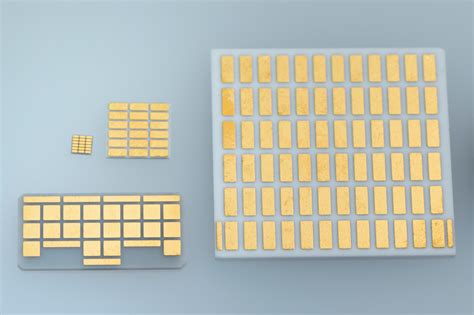
Common Ceramic PCB Materials
Several ceramic materials are used in the manufacturing of ceramic PCBs, each with its own unique properties and advantages:
1. Alumina (Al2O3)
Alumina is the most widely used ceramic material for PCBs due to its excellent electrical insulation properties, good thermal conductivity, and relatively low cost compared to other ceramic materials. It is available in various purities, with 96% and 99.5% being the most common.
2. Aluminum Nitride (AlN)
Aluminum nitride offers superior thermal conductivity compared to alumina, making it an excellent choice for high-power applications that require efficient heat dissipation. It also has a low dielectric constant and loss tangent, making it suitable for high-frequency applications.
3. Beryllium Oxide (BeO)
Beryllium oxide has the highest thermal conductivity among ceramic PCB materials, making it ideal for extremely high-power applications. However, BeO is toxic in powder form, which makes it less common and more expensive than other ceramic materials.

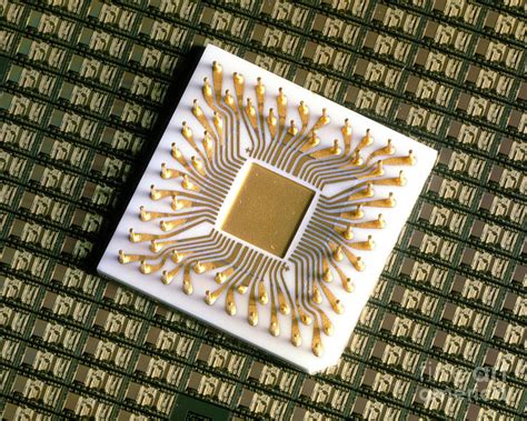
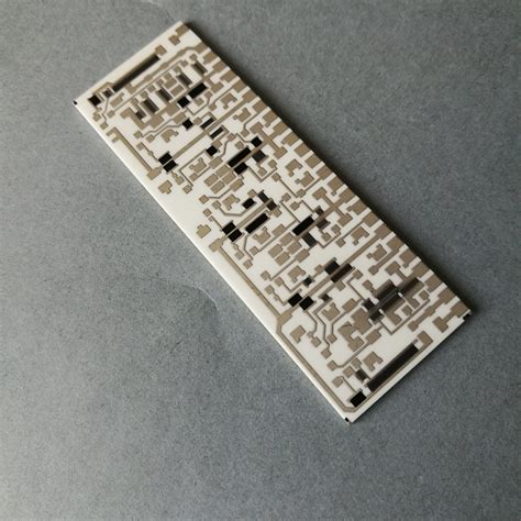
Manufacturing Process for Ceramic PCBs
The manufacturing process for ceramic PCBs differs from that of traditional FR-4 PCBs and typically involves the following steps:
-
Ceramic Substrate Preparation: The ceramic substrate is formed by mixing ceramic powders with binders and pressing the mixture into the desired shape.
-
Green Machining: The pressed ceramic substrate, known as a “green” substrate, is machined to create vias, holes, and other features.
-
Sintering: The green substrate is fired in a high-temperature furnace to sinter the ceramic particles together, creating a dense and strong substrate.
-
Metallization: Conductive traces and pads are applied to the ceramic substrate using thin-film or thick-film deposition techniques, such as screen printing, sputtering, or plating.
-
Patterning: The metallized substrate is patterned using photolithography and etching processes to define the desired circuit layout.
-
Inspection and Testing: The completed ceramic PCB undergoes thorough inspection and electrical testing to ensure it meets the required specifications.
Applications of Ceramic PCBs
Ceramic PCBs find use in a wide range of industries and applications where their unique properties are essential:
- Aerospace and Defense:
- Radar systems
- Satellite communications
-
Avionics
-
Automotive:
- Engine control units
- High-temperature sensors
-
Electric vehicle power electronics
-
Medical:
- Implantable devices
- Surgical instruments
-
Diagnostic equipment
-
Industrial:
- Oil and gas exploration
- Power electronics
-
High-temperature process control
-
Telecommunications:
- 5G wireless infrastructure
- Microwave circuits
- High-frequency filters and amplifiers
Frequently Asked Questions (FAQ)
1. Can ceramic PCBs be multilayer?
Yes, ceramic PCBs can be manufactured as multilayer boards, allowing for more complex circuit designs and higher component density. However, the number of layers is typically limited compared to FR-4 PCBs due to the more complex manufacturing process.
2. Are ceramic PCBs more environmentally friendly than FR-4 PCBs?
Ceramic PCBs can be considered more environmentally friendly than FR-4 PCBs in certain aspects. They do not contain the same flame retardants and other potentially harmful chemicals used in FR-4 manufacturing. Additionally, the high durability and reliability of ceramic PCBs can lead to longer product lifetimes, reducing electronic waste.
3. How do the electrical properties of ceramic PCBs compare to FR-4?
Ceramic PCBs generally have lower dielectric constants and loss tangents compared to FR-4, which makes them more suitable for high-frequency applications. They also offer better insulation resistance and higher breakdown voltages.
4. Can ceramic PCBs be used in consumer electronics?
While ceramic PCBs offer many advantages, their higher cost and limited design flexibility make them less common in consumer electronics. They are more often used in specialized, high-performance applications where their unique properties justify the increased cost.
5. Are there any special considerations for assembling components on ceramic PCBs?
Yes, the brittle nature of ceramic PCBs requires special care during component assembly. Techniques such as low-stress mounting, using compliant lead materials, and controlling the thermal gradient during soldering can help minimize the risk of damage to the ceramic substrate.
In conclusion, ceramic PCBs offer a range of unique properties that make them an essential choice for high-performance applications across various industries. While they may have higher costs and some design limitations compared to traditional FR-4 PCBs, their ability to withstand extreme temperatures, provide excellent electrical insulation, and offer superior thermal conductivity makes them indispensable in demanding environments.
As technology continues to advance, the use of ceramic PCBs is likely to grow in areas such as 5G telecommunications, electric vehicles, and aerospace electronics. By understanding the advantages, disadvantages, and applications of ceramic PCBs, engineers and designers can make informed decisions when selecting the most appropriate circuit board material for their projects.
Leave a Reply