Introduction to PCB-BOM
Printed Circuit Boards (PCBs) are essential components in modern electronics. They provide a platform for mounting and connecting various electronic components, enabling the creation of complex circuits. When designing and manufacturing PCBs, one crucial aspect is the Bill of Materials (BOM). The BOM is a comprehensive list of all the components required to assemble a PCB, including their quantities, part numbers, and specifications. Accurate BOM statistics data is vital for ensuring the successful fabrication and assembly of PCBs.
In this article, we will guide you through the process of building your own PCBs using clear instructions derived from accurate BOM statistics data. We will cover the importance of BOM accuracy, the steps involved in creating a PCB, and provide valuable insights to help you streamline your PCB design and manufacturing process.
The Importance of Accurate BOM Statistics Data
Ensuring Component Availability
One of the primary reasons for maintaining accurate BOM statistics data is to ensure the availability of all required components. By having a precise list of components, along with their quantities and specifications, you can effectively plan your procurement process. This helps avoid delays caused by out-of-stock components or long lead times, which can significantly impact your project timeline.
Cost Optimization
Accurate BOM statistics data enables you to optimize the cost of your PCB project. By having a clear understanding of the components required and their respective prices, you can make informed decisions regarding component selection. You can identify opportunities for cost savings by choosing alternative components with similar functionality or by negotiating better prices with suppliers based on the quantities needed.
Avoiding Assembly Errors
A well-maintained BOM ensures that the PCB assembly process is accurate and efficient. It provides clear instructions to the assembly team, specifying the exact components to be placed on the board and their locations. This reduces the risk of assembly errors, such as missing components or incorrect placements, which can lead to functionality issues or delays in the manufacturing process.
Steps to Build Your Own PCBs
Step 1: PCB Design
The first step in building your own PCBs is to create a comprehensive design. This involves selecting the appropriate components, determining their placement on the board, and routing the connections between them. There are various PCB design software tools available, such as Altium Designer, Eagle, or KiCad, which provide user-friendly interfaces and extensive libraries of components.
When designing your PCB, consider the following factors:
- Component selection: Choose components that meet your functional requirements, power ratings, and form factors.
- Schematic design: Create a schematic diagram that represents the logical connections between components.
- Board layout: Determine the physical placement of components on the board, considering factors such as signal integrity, thermal management, and manufacturability.
- Design rules: Adhere to the design rules and guidelines provided by your chosen PCB manufacturer to ensure compatibility and reliability.
Step 2: BOM Creation
Once your PCB design is complete, the next step is to generate an accurate BOM. The BOM should include the following information for each component:
- Part number or reference designator
- Quantity required
- Description or value
- Package type or footprint
- Manufacturer and supplier information
To create a comprehensive BOM, follow these guidelines:
- Review your schematic and board layout to ensure all components are accounted for.
- Use consistent naming conventions and part numbers to avoid confusion.
- Verify the availability and lead times of components with your suppliers.
- Include any additional materials required for assembly, such as solder paste or mounting hardware.
Here’s an example of a simple BOM table:
| Reference | Quantity | Description | Package | Manufacturer |
|---|---|---|---|---|
| R1, R2 | 2 | 10kΩ Resistor | 0805 | Yageo |
| C1 | 1 | 10μF Capacitor | 0603 | Murata |
| U1 | 1 | ATmega328P | TQFP-32 | Microchip |
| D1 | 1 | LED | 0805 | Kingbright |
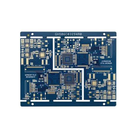
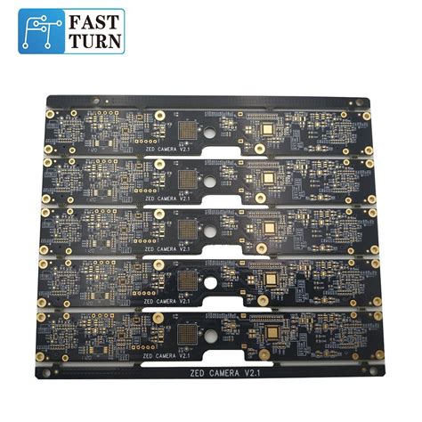
Step 3: PCB Fabrication
With your PCB design and BOM ready, the next step is to send them to a PCB fabrication service. There are numerous PCB manufacturers available, both locally and online, that offer a range of fabrication options.
When selecting a PCB fabricator, consider the following factors:
- Manufacturing capabilities: Ensure the fabricator can handle your specific PCB requirements, such as the number of layers, material type, and surface finish.
- Turnaround time: Consider the fabrication lead time and how it aligns with your project timeline.
- Pricing: Compare prices from multiple fabricators to find the best value for your project budget.
- Quality and reliability: Look for fabricators with a good reputation and track record of delivering high-quality PCBs.
Once you have selected a fabricator, provide them with your PCB design files (usually in Gerber format) and BOM. They will review your files, provide feedback if necessary, and proceed with the fabrication process.
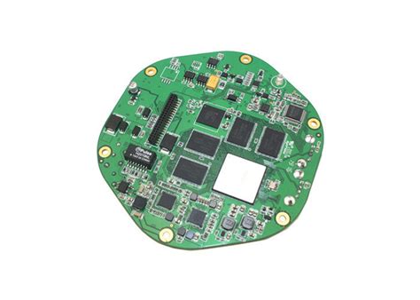
Step 4: PCB Assembly
After receiving the fabricated PCBs, the final step is to assemble the components onto the board. You can choose to assemble the PCBs yourself or outsource the assembly to a professional assembly service.
If you decide to assemble the PCBs yourself, follow these steps:
- Gather the necessary tools and equipment, such as soldering iron, solder, tweezers, and magnifying glass.
- Refer to your BOM and PCB layout to determine the placement of each component.
- Apply solder paste to the pads on the PCB using a stencil or syringe.
- Place the components onto the pads, ensuring correct orientation and alignment.
- Reflow the solder paste using a reflow oven or hot air gun to establish secure connections.
- Inspect the assembLED PCB for any soldering defects or misaligned components.
- Perform functional testing to verify the operation of the assembled PCB.
If you choose to outsource the assembly, provide the assembly service with your fabricated PCBs, BOM, and any specific assembly instructions. They will handle the component procurement and assembly process based on your requirements.

Frequently Asked Questions (FAQ)
-
Q: What is the difference between a schematic and a PCB layout?
A: A schematic is a graphical representation of the electrical connections and components in a circuit, while a PCB layout depicts the physical arrangement of those components on the actual printed circuit board. -
Q: How do I ensure the accuracy of my BOM?
A: To ensure BOM accuracy, thoroughly review your schematic and PCB layout, cross-reference component information with supplier data, and use consistent naming conventions. It’s also helpful to have a peer or colleague review your BOM for any discrepancies. -
Q: Can I modify my PCB design after sending it for fabrication?
A: Once you have sent your PCB design files to the fabricator, making changes becomes more difficult and costly. It’s essential to thoroughly review and validate your design before submitting it for fabrication to avoid the need for modifications. -
Q: How do I choose the right components for my PCB?
A: When selecting components, consider factors such as functionality, power ratings, package types, and availability. Refer to datasheets and application notes to ensure compatibility with your circuit requirements. It’s also important to consider the cost and lead times of components to align with your project budget and timeline. -
Q: What are some common PCB assembly defects to watch out for?
A: Common PCB assembly defects include solder bridges (unintended connections between pads), cold solder joints (poor solder connections), component misalignment, and missing or incorrectly placed components. Thorough visual inspection and functional testing can help identify and rectify these defects.
Conclusion
Building your own PCBs can be a rewarding and cost-effective approach to bringing your electronic designs to life. By following clear instructions derived from accurate BOM statistics data, you can streamline the PCB design, fabrication, and assembly process.
Remember to prioritize accuracy in your BOM creation, carefully select components and fabrication partners, and pay attention to detail during the assembly stage. By adhering to best practices and leveraging the right tools and resources, you can successfully create high-quality PCBs that meet your project requirements.
As you embark on your PCB building journey, continuously refine your skills, stay updated with industry trends, and don’t hesitate to seek guidance from experienced professionals when needed. With practice and perseverance, you’ll be able to create increasingly complex and sophisticated PCBs that power innovative electronic projects.
Leave a Reply