Introduction to High-Speed Design
High-speed design is a specialized field within electronic engineering that focuses on the design and development of electronic systems capable of operating at high frequencies and data rates. As technology advances and the demand for faster, more efficient electronic devices increases, high-speed design has become increasingly important in various industries, such as telecommunications, computing, and automotive.
In this comprehensive article, we will delve into the world of high-speed design, exploring its fundamental concepts, challenges, and best practices. We will also discuss the tools and techniques used by engineers to overcome the unique obstacles associated with designing high-speed electronic systems.
Key Aspects of High-Speed Design
- Signal Integrity
- Power Integrity
- Electromagnetic Compatibility (EMC)
- Thermal Management
- Board Layout and Routing
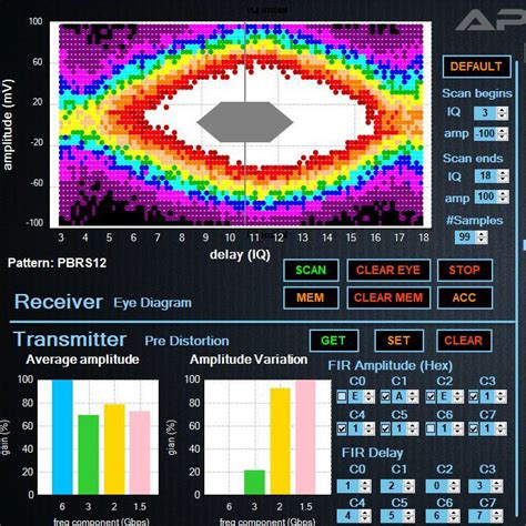
Signal Integrity in High-Speed Design
Signal integrity is a critical aspect of high-speed design, as it directly impacts the quality and reliability of the electronic system. At high frequencies, signals are more susceptible to various phenomena that can degrade their quality, such as:
- Reflections
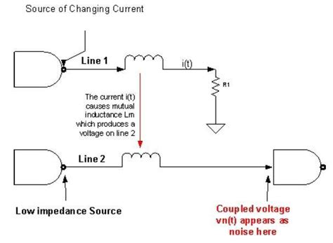
- Crosstalk
- Attenuation
- Dispersion
To maintain signal integrity, engineers must carefully consider factors such as impedance matching, termination, and transmission line effects. Proper design techniques, such as controlled impedance routing, differential signaling, and equalization, can help mitigate signal integrity issues.
Common Signal Integrity Issues and Solutions
| Issue | Description | Solution |
|---|---|---|
| Reflections | Signal reflections occur when there is an impedance mismatch along the transmission path. | – Impedance matching – Proper termination – Controlled impedance routing |
| Crosstalk | Crosstalk is the unwanted coupling of signals between adjacent traces or wires. | – Increased spacing between traces – Differential signaling – Shielding |
| Attenuation | Attenuation is the loss of signal strength as it travels along the transmission path. | – Equalization techniques – Low-loss materials – Shorter trace lengths |
| Dispersion | Dispersion is the spreading of a signal in time due to frequency-dependent propagation velocities. | – Material selection – Controlled dielectric thickness – Equalization techniques |
Power Integrity in High-Speed Design
Power integrity is another crucial aspect of high-speed design, as it ensures that the electronic components receive a clean, stable power supply. At high frequencies, the power delivery network (PDN) can be affected by various issues, such as:
- Voltage drop
- Ground bounce
- Simultaneous switching noise (SSN)
To maintain power integrity, engineers must design a robust PDN that minimizes impedance and provides adequate decoupling. Techniques such as power plane segmentation, decoupling capacitor placement, and low-inductance packaging can help improve power integrity.
Power Integrity Design Techniques
- Power plane segmentation
- Separating power planes for different voltage domains
-
Minimizing the interaction between high-speed and low-speed circuits
-
Decoupling capacitor placement
- Placing decoupling capacitors close to the power pins of ICs
-
Using a combination of bulk and ceramic capacitors for broadband decoupling
-
Low-inductance packaging
- Selecting packages with low-inductance power and ground connections
- Using ball grid array (BGA) packages for improved power delivery

Electromagnetic Compatibility (EMC) in High-Speed Design
Electromagnetic compatibility (EMC) is the ability of an electronic system to operate properly in its electromagnetic environment without causing or being susceptible to electromagnetic interference (EMI). In high-speed design, EMC is a significant challenge due to the increased likelihood of EMI at high frequencies.
To ensure EMC, engineers must consider both the emission and susceptibility of the electronic system. Techniques such as proper grounding, shielding, and filtering can help minimize EMI and improve the overall EMC of the system.
EMC Design Techniques
- Proper grounding
- Implementing a low-impedance ground plane
- Using a star grounding scheme for low-frequency signals
-
Employing a grid or mesh grounding scheme for high-frequency signals
-
Shielding
- Using metallic enclosures to contain EMI
- Applying shielding materials to cables and connectors
-
Implementing on-board shielding for sensitive components
-
Filtering
- Applying low-pass, high-pass, or band-pass filters to limit EMI
- Using Ferrite Beads or chokes to suppress high-frequency noise
- Implementing power supply filtering to reduce conducted EMI
Thermal Management in High-Speed Design
Thermal management is an essential aspect of high-speed design, as electronic components generate heat during operation. At high frequencies, the power dissipation of components increases, leading to higher heat generation. Proper thermal management is necessary to ensure the reliability and longevity of the electronic system.
To manage heat effectively, engineers must consider factors such as component placement, airflow, and heat sinking. Techniques such as thermal simulation, temperature monitoring, and active cooling can help optimize the thermal performance of the system.
Thermal Management Techniques
- Component placement
- Placing high-power components away from temperature-sensitive devices
- Arranging components to promote natural convection
-
Considering the thermal coupling between components
-
Airflow management
- Designing enclosures with proper venting and airflow paths
- Using fans or blowers to force air through the system
-
Implementing air baffles or ducts to direct airflow over critical components
-
Heat sinking
- Attaching heat sinks to high-power components
- Selecting heat sink materials with high thermal conductivity
-
Optimizing heat sink geometry for maximum heat dissipation
-
Thermal simulation
- Using computational fluid dynamics (CFD) tools to model airflow and temperature distribution
- Performing thermal simulations early in the design process to identify potential issues
- Validating thermal simulations with physical measurements
Board Layout and Routing in High-Speed Design
Board layout and routing are critical aspects of high-speed design, as they directly impact signal integrity, power integrity, and EMC. Proper layout and routing techniques can help minimize the effects of high-frequency phenomena and ensure the optimal performance of the electronic system.
When designing high-speed PCBs, engineers must consider factors such as trace geometry, layer stackup, and component placement. Techniques such as controlled impedance routing, differential pair routing, and length matching can help maintain signal integrity and minimize crosstalk.
High-Speed PCB Layout and Routing Techniques
- Controlled impedance routing
- Designing traces with specific width and spacing to achieve the desired characteristic impedance
- Using PCB stackup materials with consistent Dielectric Properties
-
Maintaining a constant trace width and spacing throughout the signal path
-
Differential pair routing
- Routing differential signals as closely-spaced pairs to minimize crosstalk and EMI
- Maintaining equal length and symmetry between the positive and negative traces
-
Using serpentine or delay line techniques to match the length of differential pairs
-
Length matching
- Ensuring that the length of all traces in a bus or group are matched within a specified tolerance
- Using serpentine or delay line techniques to adjust trace lengths
-
Considering the impact of via stubs on signal propagation delay
-
Component placement
- Placing components to minimize the length of high-speed traces
- Grouping components with similar functions or signal speeds
- Considering the orientation of components to optimize routing and minimize crosstalk
Tools and Techniques for High-Speed Design
To successfully design and analyze high-speed electronic systems, engineers rely on a variety of tools and techniques. These tools help simulate, measure, and optimize the performance of the system, ensuring that it meets the desired specifications and standards.
High-Speed Design Tools
- Electronic Design Automation (EDA) software
- Schematic capture and PCB layout tools
- Signal and power integrity simulation tools
-
Electromagnetic field solvers for EMC analysis
-
Measurement and test equipment
- High-bandwidth oscilloscopes
- Vector network analyzers (VNAs)
- Spectrum analyzers
-
Time-domain reflectometers (TDRs)
-
Prototyping and validation
- Rapid prototyping techniques, such as 3D printing and PCB milling
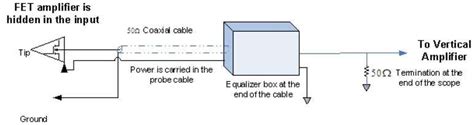
- High-speed test fixtures and probes
- Automated test equipment (ATE) for production testing
High-Speed Design Techniques
- Pre-layout simulation
- Performing signal and power integrity simulations before PCB layout
- Optimizing component selection and placement based on simulation results
-
Identifying potential issues early in the design process
-
Post-layout verification
- Running signal and power integrity simulations on the final PCB layout
- Verifying that the design meets the required specifications and standards
-
Identifying and correcting any issues before prototyping or production
-
Measurement and validation
- Performing laboratory measurements on prototypes or production units
- Validating simulation results with physical measurements
- Identifying and troubleshooting any discrepancies between simulations and measurements
Real-World Applications of High-Speed Design
High-speed design is essential in various industries and applications where high-frequency operation and fast data transfer are required. Some examples of real-world applications that rely on high-speed design include:
- Telecommunications
- 5G wireless networks
- Fiber-optic communication systems
-
Satellite communication systems
-
Computing
- High-performance computing (HPC) systems
- Data centers and server farms
-
Graphics processing units (GPUs) and accelerators
-
Automotive
- Advanced driver assistance systems (ADAS)
- In-vehicle infotainment systems
-
Vehicle-to-vehicle (V2V) and vehicle-to-infrastructure (V2I) communication
-
Medical
- High-resolution medical imaging systems
- Wireless medical devices and sensors
-
Telemedicine and remote patient monitoring
-
Aerospace and Defense
- Radar and surveillance systems
- Satellite communication and navigation systems
- Avionics and flight control systems
In each of these applications, high-speed design plays a crucial role in ensuring the reliable, efficient, and robust operation of electronic systems in demanding environments.
Challenges and Future Trends in High-Speed Design
As technology continues to advance and the demand for higher speeds and data rates increases, high-speed design faces several challenges and opportunities. Some of the key challenges and future trends in high-speed design include:
Challenges
- Increasing signal speeds and frequencies
- Designing for higher data rates and clock frequencies
- Managing increased signal integrity and power integrity issues
-
Dealing with more pronounced high-frequency effects, such as skin effect and dielectric loss
-
Miniaturization and higher density
- Designing for smaller form factors and higher component densities
- Managing increased thermal and mechanical challenges
-
Dealing with more complex signal routing and layer stackups
-
Power consumption and efficiency
- Designing for lower power consumption and higher efficiency
- Managing power integrity and thermal challenges in high-density designs
- Implementing advanced power management techniques, such as dynamic voltage and frequency scaling (DVFS)
Future Trends
- Advanced packaging technologies
- Implementing 2.5D and 3D packaging techniques, such as interposers and through-silicon vias (TSVs)
- Using advanced materials, such as low-loss dielectrics and high-conductivity metals
-
Exploring novel packaging concepts, such as embedded components and wafer-level packaging
-
Photonic and optical interconnects
- Integrating photonic and optical components into high-speed designs
- Using optical interconnects for high-bandwidth, low-latency communication
-
Developing hybrid electrical-optical PCBs and packaging solutions
-
Artificial intelligence and machine learning
- Applying AI and ML techniques to high-speed design automation and optimization
- Using AI-driven tools for signal and power integrity analysis and prediction
- Implementing AI accelerators and processors in high-speed systems for edge computing and inferencing
As high-speed design continues to evolve, engineers will need to stay up-to-date with the latest tools, techniques, and best practices to overcome these challenges and take advantage of emerging opportunities.
Frequently Asked Questions (FAQ)
- What is the difference between signal integrity and power integrity in high-speed design?
-
Signal integrity focuses on maintaining the quality and fidelity of high-speed signals as they propagate through the system, while power integrity focuses on ensuring a clean, stable power supply to the electronic components. Both are critical for the proper operation of high-speed systems.
-
Why is EMC important in high-speed design?
-
EMC is important in high-speed design because high-frequency signals are more susceptible to causing and being affected by electromagnetic interference (EMI). Ensuring EMC helps prevent the electronic system from interfering with other devices and being disrupted by external EMI sources.
-
How does thermal management impact high-speed design?
-
Proper thermal management is crucial in high-speed design because electronic components generate more heat at higher frequencies. Overheating can lead to reduced performance, reliability issues, and even device failure. Effective thermal management helps ensure the long-term stability and reliability of high-speed systems.
-
What are some common PCB layout and routing techniques used in high-speed design?
-
Common PCB layout and routing techniques in high-speed design include controlled impedance routing, differential pair routing, and length matching. These techniques help maintain signal integrity, minimize crosstalk, and ensure proper timing and synchronization of high-speed signals.
-
What are some emerging trends in high-speed design?
- Some emerging trends in high-speed design include advanced packaging technologies, such as 2.5D and 3D packaging, photonic and optical interconnects for high-bandwidth communication, and the application of artificial intelligence and machine learning techniques for design automation and optimization.
Conclusion
High-speed design is a critical aspect of modern electronic engineering, enabling the development of faster, more efficient, and more reliable electronic systems. As technology continues to advance, the importance of high-speed design will only continue to grow, driving innovation in various industries and applications.
In this article, we have explored the fundamental concepts, challenges, and best practices of high-speed design, covering topics such as signal integrity, power integrity, EMC, thermal management, and board layout and routing. We have also discussed the tools and techniques used by engineers to overcome the unique challenges associated with designing high-speed electronic systems.
By understanding the principles and techniques of high-speed design, engineers can create electronic systems that push the boundaries of performance and functionality, enabling new applications and technologies that shape our world.
Leave a Reply