Step 1: Define Your PCB’s Purpose and Requirements
Before you start designing your PCB, it’s essential to have a clear understanding of its purpose and the specific requirements it needs to meet. Consider the following factors:
- The function of the PCB (e.g., power supply, sensor board, microcontroller)
- The components required (e.g., resistors, capacitors, ICs)
- The size and shape constraints
- The environmental conditions (e.g., temperature, humidity, vibration)
- The power requirements and voltage levels
- The required connectors and interfaces
By defining these factors upfront, you’ll have a solid foundation for your PCB design and avoid potential issues down the line.
Step 2: Create a Schematic Diagram
A schematic diagram is a graphical representation of your PCB’s electronic circuits. It shows how the components are connected and helps you visualize the flow of electricity through the board. To create a schematic diagram:
- Choose a schematic capture tool (e.g., Eagle, KiCad, Altium Designer)
- Place the required components on the schematic canvas
- Connect the components using wires or nets
- Assign unique identifiers to each component (e.g., R1 for a resistor, C1 for a capacitor)
- Add power and ground symbols
- Double-check your connections and ensure the schematic is accurate
Step 3: Select Your PCB’s Form Factor and Dimensions
With your schematic diagram complete, it’s time to decide on your PCB’s form factor and dimensions. Consider the following factors:
- The available space in the enclosure or device
- The number and size of components
- The required mounting holes and mechanical features
- The desired thickness of the PCB (typically 1.6mm for most applications)
Common PCB form factors include:
| Form Factor | Dimensions (mm) | Typical Applications |
|---|---|---|
| Arduino Uno | 68.6 x 53.4 | Prototyping, hobbyist projects |
| Raspberry Pi | 85 x 56 | Single-board computers, IoT |
| Credit Card | 85.6 x 54 | Wearables, portable devices |
| Eurocircuits 5x5cm | 50 x 50 | Small, compact designs |

Step 4: Choose Your PCB Layering and Material
PCBs can have anywhere from one to multiple layers, depending on the complexity of the design and the routing requirements. The most common PCB layering options are:
- Single-sided: Components and traces on one side only
- Double-sided: Components and traces on both sides
- Multi-layer: Four or more layers, with internal layers for power and ground planes
The choice of PCB material is also important, as it affects the board’s electrical and mechanical properties. The most common PCB materials are:
- FR-4: A glass-reinforced epoxy laminate, suitable for most applications
- Rogers: A high-frequency laminate with low dielectric loss, used for RF and microwave designs
- Aluminum: A metal-core PCB that provides excellent heat dissipation
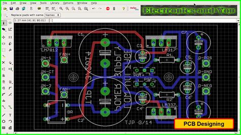
Step 5: Place Your Components on the PCB Layout
With your schematic, form factor, and layering choices made, it’s time to start placing components on the PCB layout. Using a PCB layout tool (such as Eagle or KiCad), follow these steps:
- Import your schematic diagram into the PCB layout tool
- Define the board outline and any mechanical features (e.g., mounting holes)
- Place the components on the board, keeping in mind:
- Proper orientation and spacing
- Thermal considerations for heat-generating components
- Electromagnetic interference (EMI) and signal integrity
- Ensure all components are properly labeled and identified
Step 6: Route the Traces and Copper Pours
With your components placed, it’s time to route the traces that connect them electrically. Traces are the copper pathways that carry signals and power between components. When routing traces, consider:
- Trace width: Wider traces can carry more current and have lower resistance
- Trace spacing: Adequate spacing between traces helps prevent short circuits and reduces crosstalk
- Trace angles: Use 45-degree angles instead of 90-degree angles to avoid sharp corners that can cause signal reflections
In addition to traces, you can also add copper pours (also known as fills) to your PCB design. Copper pours are large areas of copper that provide a low-impedance path for power and ground connections, as well as helping with heat dissipation and EMI reduction.
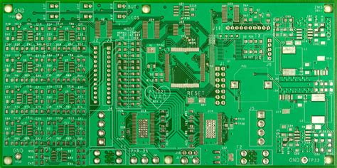
Step 7: Add Silkscreen and Solder Mask Layers
Silkscreen and solder mask layers are important for the aesthetics and usability of your PCB. The silkscreen layer is used to add text, logos, and component identifiers to the PCB surface. This helps with assembly and troubleshooting. The solder mask layer is a protective coating that covers the copper traces, leaving only the pads exposed for soldering.
When adding silkscreen and solder mask layers:
- Ensure the text is legible and properly oriented
- Keep the silkscreen away from pads and other conductive areas
- Choose a contrasting color for the silkscreen (usually white on a green solder mask)
- Define the solder mask openings around pads and vias
Step 8: Generate Manufacturing Files
Once your PCB design is complete, it’s time to generate the files needed for manufacturing. The most common manufacturing files are:
- Gerber files: A set of files that describe the copper layers, solder mask, silkscreen, and drill holes
- Drill files: A file that specifies the location, size, and type of drill holes
- Bill of Materials (BOM): A list of all the components used in the design, including their quantities and part numbers
Most PCB layout tools have built-in features for generating these files. Be sure to double-check the files for accuracy before sending them to a PCB manufacturer.
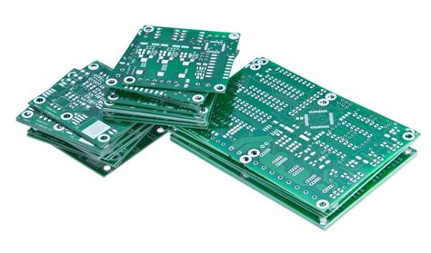
Step 9: Choose a PCB Manufacturer and Place Your Order
With your manufacturing files ready, it’s time to choose a PCB manufacturer and place your order. When selecting a manufacturer, consider:
- Cost: Get quotes from multiple manufacturers and compare prices
- Turnaround time: How quickly do you need your PCBs?
- Quality: Look for manufacturers with good reviews and a track record of producing high-quality boards
- Capabilities: Can the manufacturer handle your specific requirements (e.g., board thickness, material, finish)?
Once you’ve chosen a manufacturer, place your order and provide them with your manufacturing files. Be sure to specify any special requirements or instructions.
Step 10: Assemble and Test Your PCB
When your PCBs arrive from the manufacturer, it’s time to assemble and test them. If you’re assembling the boards yourself, follow these steps:
- Gather the necessary tools (e.g., soldering iron, solder, tweezers)
- Place the components on the board, ensuring proper orientation
- Solder the components to the pads, using proper soldering techniques
- Inspect the board for any soldering defects or misplaced components
After assembly, it’s crucial to test your PCB to ensure it functions as intended. This can involve:
- Visual inspection for any obvious defects or issues
- Continuity testing to verify proper connections between components
- Functional testing to ensure the PCB performs its intended function
- Stress testing to check the PCB’s performance under various conditions (e.g., temperature, voltage)
By thoroughly testing your PCB, you can identify and address any issues before the board goes into production or use.
Frequently Asked Questions (FAQ)
- What software do I need for PCB design?
There are many PCB Design Software options available, both free and paid. Some popular choices include: - Eagle (free for non-commercial use)
- KiCad (open-source and free)
- Altium Designer (paid, industry-standard)
-
Autodesk Fusion 360 (paid, with a free hobbyist license)
-
How much does it cost to manufacture a PCB?
The cost of PCB manufacturing depends on several factors, such as: - Board size and complexity
- Number of layers
- Material and finish
-
Quantity ordered
Prices can range from a few dollars per board for small, simple designs to hundreds of dollars for large, complex boards. Many manufacturers offer online quoting tools to help estimate costs. -
What are the most common PCB manufacturing techniques?
The two most common PCB manufacturing techniques are: - Through-hole technology (THT): Components have leads that are inserted into holes drilled in the board and soldered on the opposite side.
-
Surface-mount technology (SMT): Components are mounted directly onto the surface of the board, with no leads penetrating through the board.
-
What are some common PCB design mistakes to avoid?
Some common PCB design mistakes include: - Incorrect component orientation or placement
- Insufficient trace width or spacing
- Lack of proper grounding or power distribution
- Ignoring thermal considerations for heat-generating components
-
Neglecting EMI and signal integrity issues
By being aware of these potential pitfalls and following best practices, you can avoid costly mistakes in your PCB design. -
How long does it take to design and manufacture a PCB?
The time required to design and manufacture a PCB can vary widely depending on the complexity of the design and the manufacturer’s turnaround time. A simple, single-layer board may take just a few hours to design and a few days to manufacture, while a complex, multi-layer board can take weeks or even months to design and manufacture.
To minimize design time, it’s important to have a clear plan and well-defined requirements from the start. Using a modular design approach and leveraging existing libraries and templates can also help speed up the design process. When selecting a manufacturer, be sure to consider their turnaround time and communicate your timeline requirements clearly.
Conclusion
Designing a PCB can seem like a complex and intimidating process, but by following these 10 easy steps, you can create a functional and professional-looking board. Remember to start with a clear understanding of your PCB’s purpose and requirements, create a detailed schematic diagram, and carefully consider your component placement and routing. Don’t forget to add silkscreen and solder mask layers, generate accurate manufacturing files, and thoroughly test your assembled board.
With practice and persistence, you’ll soon be designing PCBs like a pro. Happy designing!
Leave a Reply