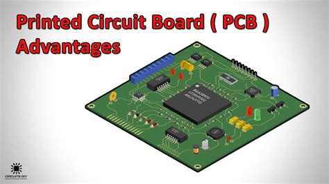
Introduction to PCBs and their applications
Printed Circuit Boards (PCBs) are the backbone of modern electronics. They are used in almost every electronic device we use today, from smartphones and computers to medical equipment and aerospace systems. PCBs are essential because they provide a reliable and efficient way to connect electronic components and create complex circuits.
In this article, we will explore the reasons why PCBs are used, their benefits, and their applications in various industries. We will also discuss the different types of PCBs and their manufacturing process.
What are PCBs?
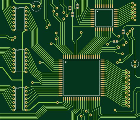
PCBs are flat boards made of insulating materials, such as fiberglass or plastic, with conductive tracks printed on them. These tracks are made of copper and are used to connect electronic components, such as resistors, capacitors, and integrated circuits (ICs), to form a complete circuit.
PCBs come in different sizes and shapes, depending on the application they are used for. They can be single-sided, double-sided, or multi-layered, with each layer containing its own set of conductive tracks.
Benefits of using PCBs
1. Compact size
One of the main advantages of using PCBs is their compact size. PCBs allow for the miniaturization of electronic devices by providing a way to densely pack electronic components onto a small board. This is especially important in modern electronics, where devices are becoming smaller and more portable.
For example, smartphones today are much smaller than they were a decade ago, yet they contain more features and functionality. This is made possible by the use of PCBs, which allow for the integration of multiple components onto a single board.
2. Reliability
PCBs are highly reliable compared to other methods of connecting electronic components, such as point-to-point wiring. The conductive tracks on PCBs are designed to provide a stable and secure connection between components, reducing the risk of short circuits and other electrical faults.
Moreover, PCBs are manufactured using automated processes, which ensure consistency and accuracy in the placement of components and the routing of tracks. This reduces the likelihood of human error and improves the overall reliability of the circuit.
3. Cost-effective
Using PCBs is also cost-effective, especially for mass production. Once the initial design and setup costs are covered, PCBs can be manufactured in large quantities at a relatively low cost per unit.
In contrast, point-to-point wiring is labor-intensive and time-consuming, making it unsuitable for mass production. It also requires more materials, such as wires and connectors, which adds to the overall cost of the device.
4. Easier troubleshooting and repair
PCBs make it easier to troubleshoot and repair electronic devices. The conductive tracks on PCBs are clearly visible, making it easy to trace the flow of electricity and identify any faults or defects.
Additionally, PCBs are designed with testability in mind. They often include test points and other features that allow for easy testing and debugging of the circuit.
5. Better signal integrity
PCBs provide better signal integrity compared to other methods of connecting electronic components. The conductive tracks on PCBs are designed to minimize electromagnetic interference (EMI) and crosstalk, which can degrade the quality of the signal.
Moreover, PCBs can be designed with controlled impedance, which ensures that the signal maintains its integrity as it travels through the circuit. This is particularly important in high-speed applications, such as telecommunications and data transmission.

Applications of PCBs
PCBs are used in a wide range of industries and applications. Some of the most common applications include:
1. Consumer electronics
PCBs are used in almost every consumer electronic device, from smartphones and laptops to televisions and gaming consoles. They provide a compact and reliable way to connect the various components that make up these devices.
| Device | PCB Usage |
|---|---|
| Smartphone | Main board, display board, camera module, sensors |
| Laptop | Motherboard, display board, touchpad, keyboard controller |
| Television | Main board, power supply board, backlight board |
| Gaming console | Motherboard, graphics card, power supply board |
2. Automotive electronics
PCBs are extensively used in automotive electronics, from engine control units (ECUs) to infotainment systems. They provide a rugged and reliable solution for connecting electronic components in the harsh automotive environment.
| Application | PCB Usage |
|---|---|
| Engine control unit | Main board, sensor interfaces, power supply |
| Infotainment system | Main board, display board, audio amplifier, antenna |
| Instrument cluster | Main board, display board, sensors |
| Body control module | Main board, power distribution, relay control |
3. Medical devices
PCBs are crucial in medical devices, where reliability and accuracy are of utmost importance. They are used in a wide range of medical equipment, from patient monitors to diagnostic imaging systems.
| Device | PCB Usage |
|---|---|
| Patient monitor | Main board, sensor interfaces, power supply |
| Diagnostic imaging system | Main board, data acquisition board, power supply |
| Pacemaker | Main board, battery management, telemetry |
| Ventilator | Main board, sensor interfaces, motor control |
4. Aerospace and defense
PCBs are used in aerospace and defense applications, where they must withstand extreme environmental conditions and meet stringent reliability requirements. They are used in a variety of systems, from avionics to radar and communications equipment.
| Application | PCB Usage |
|---|---|
| Avionics | Main board, power supply, sensor interfaces, communications |
| Radar | Main board, RF board, power supply, antenna |
| Communications equipment | Main board, RF board, power amplifier, antenna |
| Missile guidance system | Main board, sensor interfaces, motor control |
5. Industrial automation
PCBs are used in industrial automation systems, such as programmable logic controllers (PLCs) and human-machine interfaces (HMIs). They provide a reliable and flexible way to connect sensors, actuators, and other devices in industrial environments.
| Application | PCB Usage |
|---|---|
| Programmable logic controller | Main board, I/O modules, power supply, communications |
| Human-machine interface | Main board, display board, touch controller, communications |
| Motor drive | Main board, power electronics, sensor interfaces |
| Sensor module | Main board, sensor interfaces, communications |
Types of PCBs
There are several types of PCBs, each with its own characteristics and applications. The most common types are:
1. Single-sided PCBs
Single-sided PCBs have conductive tracks on only one side of the board. They are the simplest and cheapest type of PCB, but they have limitations in terms of circuit complexity and component density.
Single-sided PCBs are used in low-cost consumer electronics, such as toys and simple appliances.
2. Double-sided PCBs
Double-sided PCBs have conductive tracks on both sides of the board, with connections between the two sides made using through-hole vias. They offer more design flexibility and higher component density than single-sided PCBs.
Double-sided PCBs are used in a wide range of applications, from consumer electronics to industrial automation.
3. Multi-layer PCBs
Multi-layer PCBs have more than two layers of conductive tracks, with insulating layers separating them. They offer the highest level of design flexibility and component density, but they are also the most expensive type of PCB.
Multi-layer PCBs are used in high-performance applications, such as aerospace and defense systems, where circuit complexity and signal integrity are critical.
4. Flexible PCBs
Flexible PCBs are made of flexible materials, such as polyimide, and can bend and flex without breaking. They are used in applications where the circuit needs to conform to a non-planar surface or where the device needs to be flexible.
Flexible PCBs are used in wearable electronics, medical devices, and aerospace applications.
5. Rigid-flex PCBs
Rigid-flex PCBs combine the benefits of rigid and flexible PCBs. They have rigid sections for mounting components and flexible sections for interconnections between the rigid sections.
Rigid-flex PCBs are used in applications where space is limited and where the circuit needs to be folded or bent, such as in smartphones and cameras.
PCB Manufacturing Process
The PCB manufacturing process involves several steps, from design to assembly. The main steps are:
-
Design: The circuit is designed using electronic design automation (EDA) software, which generates the PCB layout files.
-
Printing: The PCB layout files are used to create a photomask, which is used to print the circuit pattern onto the copper-clad board.
-
Etching: The exposed copper is etched away, leaving only the desired circuit pattern.
-
Drilling: Holes are drilled into the board for through-hole components and vias.
-
Plating: The holes are plated with copper to create electrical connections between layers.
-
Solder mask application: A protective solder mask is applied to the board to prevent short circuits and improve the board’s appearance.
-
Silkscreen printing: Text and symbols are printed onto the board for identification and assembly purposes.
-
Surface finish application: A surface finish, such as gold or silver, is applied to the exposed copper to prevent oxidation and improve solderability.
-
Assembly: The electronic components are placed onto the board and soldered in place.
-
Testing: The assembled board is tested to ensure it functions as intended.
Frequently Asked Questions (FAQ)
1. What is the difference between a PCB and a printed wiring board (PWB)?
A PCB and a PWB are essentially the same thing. The term “printed wiring board” was used in the past, but “printed circuit board” is the more common term today.
2. Can PCBs be recycled?
Yes, PCBs can be recycled. However, the process is complex and requires specialized equipment to separate the various materials, such as copper, gold, and plastic. Many countries have regulations in place for the proper disposal and recycling of electronic waste, including PCBs.
3. What is the environmental impact of PCB manufacturing?
PCB manufacturing can have a significant environmental impact if not properly managed. The process involves the use of hazardous chemicals, such as acids and solvents, which can pollute the air, water, and soil if not disposed of properly. However, many PCB manufacturers today have implemented environmentally friendly practices, such as using lead-free solder and reducing water usage.
4. What is the future of PCB technology?
The future of PCB technology is driven by the demand for smaller, faster, and more complex electronic devices. Some of the emerging trends in PCB technology include:
- High-density interconnect (HDI) PCBs, which offer higher component density and better signal integrity
- Embedded components, where passive components are embedded within the PCB layers to save space and improve performance
- 3D printing of PCBs, which allows for the creation of complex, non-planar structures
- Flexible and stretchable PCBs, which can conform to any shape and are suitable for wearable electronics and IoT applications
5. How can I learn more about PCB design and manufacturing?
There are many resources available for learning about PCB design and manufacturing, including:
- Online courses and tutorials, such as those offered by Udemy, Coursera, and LinkedIn Learning
- Books and textbooks on PCB design and manufacturing, such as “The Circuit Designer’s Companion” by Peter Wilson and “PCB Design for Real-World EMI Control” by Bruce Archambeault
- Industry conferences and trade shows, such as PCB West and IPC APEX EXPO, where you can learn about the latest trends and technologies in PCB design and manufacturing
- Joining industry associations, such as the IPC (Association Connecting Electronics Industries), which offers training, standards, and certification programs for PCB professionals
Conclusion
In conclusion, PCBs are an essential component of modern electronics, providing a reliable and efficient way to connect electronic components and create complex circuits. They offer many benefits, including compact size, reliability, cost-effectiveness, and better signal integrity.
PCBs are used in a wide range of industries and applications, from consumer electronics to aerospace and defense. They come in different types, each with its own characteristics and applications, and are manufactured using a multi-step process that involves design, printing, etching, drilling, plating, and assembly.
As electronic devices continue to become smaller, faster, and more complex, the demand for advanced PCB technologies will only increase. Emerging trends, such as HDI PCBs, embedded components, 3D printing, and flexible and stretchable PCBs, will shape the future of PCB design and manufacturing.
If you are interested in learning more about PCBs, there are many resources available, including online courses, books, industry conferences, and associations. By staying up-to-date with the latest trends and technologies in PCB design and manufacturing, you can position yourself for success in this exciting and ever-evolving field.
Leave a Reply