How PCBs are Manufactured
The manufacturing process of a PCB starts with the design. The design is created using Electronic Design Automation (EDA) tools. These tools allow engineers to lay out the circuit schematic and then convert it into a physical representation which includes copper tracks, drill holes, solder masks, silkscreen legends, and so on.
Once the design is complete, it’s sent to a PCB fabrication house. Here are the typical steps in the manufacturing process:
-
Printing the circuit pattern onto the copper clad laminate: The circuit pattern is printed onto a photosensitive film. This film is then placed on top of the copper clad laminate and exposed to UV light. The UV light hardens the areas of the film that are clear, leaving the circuit pattern as hardened photoresist.
-
Etching: The laminate is then placed into an etching solution. This solution eats away at the copper that isn’t protected by the hardened photoresist. What’s left is the copper circuit pattern.
-
Drilling: Holes are drilled into the board to accommodate through-hole components and to provide interconnects between layers in multi-layer boards.
-
Plating: A thin layer of copper is chemically deposited onto the entire board, including the walls of the drilled holes. This ensures electrical continuity between layers.
-
Applying solder mask: A solder mask is applied to the board. This mask covers the copper traces but leaves the pads and holes exposed. It protects the copper from accidental short circuits and from oxidation.
-
Silkscreen: Finally, a silkscreen legend is applied to the board. This legend provides human-readable labels for components and connectors.
The Structure of a PCB
A PCB consists of several layers:
- Substrate: This is the base material of the PCB, usually fiberglass.
- Copper Layers: One or more thin layers of copper foil are laminated onto the substrate. These layers are etched to form the actual conducting pattern. A typical PCB has at least two copper layers: one on the top and one on the bottom.
- Solder Mask: This layer provides insulation between the copper layers and protects the copper from oxidation and short circuits.
- Silkscreen: This layer provides the legends and labels for the PCB.
Here’s a table summarizing the layers:
| Layer | Description |
|---|---|
| Substrate | The base material, usually fiberglass |
| Copper | Conducts electricity, etched to form circuit patterns |
| Solder Mask | Insulates and protects the copper layers |
| Silkscreen | Provides labels and legends |
How PCBs Work
The working principle of a PCB is straightforward: it provides a mechanical support for the electronic components and the electrical connections between these components.
The components are soldered onto the pads on the PCB. These pads are part of the copper layer and are connected to other pads and components through the etched copper traces. In this way, the PCB provides the electrical interconnections needed for the circuit to function.
In multi-layer boards, the different copper layers are connected through vias. A via is a hole that’s drilled through the board and then plated with copper to provide electrical continuity.
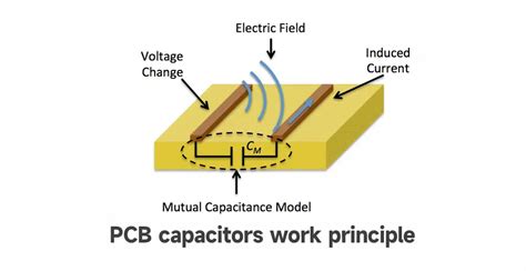
Signal integrity is a key concern in PCB design. As signals travel through the copper traces, they can be affected by factors such as:
- Resistance: The resistance of the copper traces can cause voltage drops and signal degradation.
- Capacitance: The close proximity of the traces can create parasitic capacitance, which can distort signals.
- Inductance: At high frequencies, the traces can act as inductors, causing signal reflections and EMI.
Careful design, including proper trace width, spacing, and impedance matching, is necessary to ensure signal integrity.

Types of PCBs
There are several types of PCBs, each with its own characteristics and applications:
Single Layer PCBs
Single layer PCBs have only one copper layer. They are the simplest and cheapest type of PCB, but they are limited in terms of circuit complexity and density.
Double Layer PCBs
Double layer PCBs have two copper layers, one on each side of the substrate. They allow for more complex circuits and higher component density compared to single layer boards.
Multi-Layer PCBs
Multi-layer PCBs have three or more copper layers. They allow for very complex circuits and high component density. However, they are more expensive to manufacture than single or double layer boards.
Flexible PCBs
Flexible PCBs are made with a flexible substrate, such as polyimide. They can be bent and shaped to fit into tight spaces or to connect moving parts.
Rigid-Flex PCBs
Rigid-flex PCBs are a combination of rigid and flexible PCBs. They have rigid sections for mounting components and flexible sections for connections.
Here’s a comparison table of the different types of PCBs:
| Type | Layers | Complexity | Density | Cost | Flexibility |
|---|---|---|---|---|---|
| Single Layer | 1 | Low | Low | Low | No |
| Double Layer | 2 | Medium | Medium | Medium | No |
| Multi-Layer | 3+ | High | High | High | No |
| Flexible | Varies | Varies | Varies | High | Yes |
| Rigid-Flex | Varies | High | High | Very High | Yes |
Applications of PCBs
PCBs are used in virtually all electronic devices. Some common applications include:
- Consumer Electronics: PCBs are found in TVs, smartphones, computers, gaming consoles, and more.
- Automotive: Modern cars contain many PCBs for functions such as engine control, infotainment, and driver assistance systems.
- Medical Devices: PCBs are used in a wide range of medical devices, from simple blood pressure monitors to complex imaging systems.
- Aerospace: PCBs in aerospace applications must be reliable and able to withstand harsh conditions.
- Industrial: PCBs are used in industrial control systems, power supplies, and automation equipment.
FAQ
Q: What is the difference between a PCB and a circuit board?
A: PCB stands for Printed Circuit Board. It’s a type of circuit board where the components are connected via copper traces that are printed, or “etched”, onto the board. So all PCBs are circuit boards, but not all circuit boards are PCBs. For example, a breadboard is a type of circuit board but it’s not a PCB.
Q: What is a via in a PCB?
A: A via is a hole that’s drilled through the PCB to connect different layers of copper. The hole is plated with copper to provide electrical continuity. Vias are used in multi-layer PCBs to allow signals to travel from one layer to another.
Q: What is the purpose of the solder mask on a PCB?
A: The solder mask is a layer of polymer that’s applied over the copper traces on a PCB. It serves two Main purposes: it insulates the copper traces from each other to prevent short circuits, and it protects the copper from oxidation. The solder mask is applied everywhere except on the pads where components will be soldered.
Q: Can PCBs be repaired?
A: Yes, PCBs can be repaired, but it requires skill and the right tools. Small repairs, like replacing a single component, can often be done by hand soldering. More extensive repairs may require specialized equipment like a hot air rework station. However, complex multi-layer boards can be very difficult or impossible to repair.
Q: What is the environmental impact of PCBs?
A: The manufacture of PCBs can have significant environmental impacts if not managed properly. The process involves many chemicals, including etchants, solvents, and heavy metals. Improper disposal of these chemicals can lead to environmental contamination. Additionally, the disposal of old PCBs can be problematic, as they may contain hazardous substances like lead. Proper recycling and disposal methods are necessary to minimize the environmental impact of PCBs.
In conclusion, PCBs are the backbone of modern electronics. They provide a way to mechanically support and electrically connect electronic components. The working principle of a PCB is simple, but the design and manufacture of PCBs can be complex, especially for high-density, high-speed applications. Understanding the basics of PCBs is essential for anyone involved in electronics design or manufacturing.
Leave a Reply