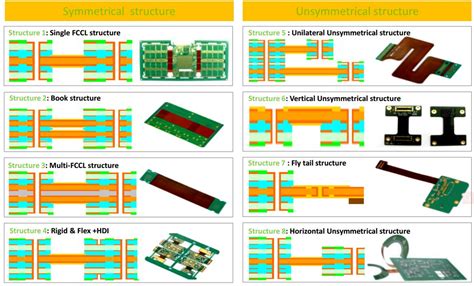
Key Elements of PCB Structure
The primary structural elements of a printed Circuit board include:
- Substrate material
- Copper layers
- Solder mask
- Silkscreen
- Vias and through-holes
- Surface finish
Substrate Material
The substrate, or base material, is the foundation of the PCB structure. It is a non-conductive, insulating layer that provides mechanical support for the copper traces and electronic components. The most common substrate materials used in PCB manufacturing are:
| Material | Description | Applications |
|---|---|---|
| FR-4 | Glass-reinforced epoxy laminate | General-purpose, high-quality PCBs |
| CEM-1 | Composite epoxy material | Low-cost, consumer-grade electronics |
| Polyimide | High-temperature, flexible polymer | Flexible and high-reliability PCBs |
| PTFE | Polytetrafluoroethylene (Teflon) | High-frequency, microwave applications |
| Alumina | Aluminum oxide ceramic | High-power, high-frequency, and high-temperature applications |
The choice of substrate material depends on the specific requirements of the application, such as thermal stability, dielectric constant, mechanical strength, and cost.
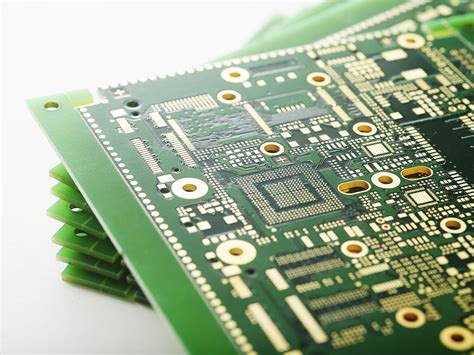
Copper Layers
Copper layers are the conductive pathways that carry electrical signals and power between components on the PCB. The number of copper layers in a PCB can vary depending on the complexity of the circuit and the routing requirements. PCBs can be classified based on the number of copper layers:
| PCB Type | Number of Copper Layers |
|---|---|
| Single-sided | 1 |
| Double-sided | 2 |
| Multi-layer | 3 or more |
The thickness of the copper layers is expressed in ounces per square foot (oz/ft²) or microns (µm). Common copper thicknesses include:
| Copper Weight | Thickness (oz/ft²) | Thickness (µm) |
|---|---|---|
| 0.5 oz | 0.0007 | 17.5 |
| 1 oz | 0.0014 | 35 |
| 2 oz | 0.0028 | 70 |
Thicker copper layers are used for high-current applications or to improve thermal dissipation.
Solder Mask
The solder mask is a protective layer applied over the copper traces on the PCB. It serves several purposes:
- Insulates copper traces to prevent short circuits
- Protects the copper from oxidation and corrosion
- Provides a surface for applying the silkscreen legend
- Improves the aesthetics of the PCB
Solder mask is typically green in color but can also be found in red, blue, black, white, or yellow. It is applied using a screen-printing process and is cured using UV light.
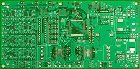
Silkscreen
The silkscreen, also known as the legend or nomenclature, is a text and symbol overlay printed on top of the solder mask. It provides important information for assembly, testing, and troubleshooting, such as:
- Component designators (e.g., R1, C2, U3)
- Polarity indicators (e.g., + and -)
- Test points and fiducial markers
- Company logos and product identifiers
Silkscreen is typically white but can also be found in black or yellow. It is applied using a screen-printing process similar to the solder mask.
Vias and Through-Holes
Vias and through-holes are used to interconnect copper layers in a multi-layer PCB. They are essential for routing signals and power between layers and components.
-
Through-holes: Drilled holes that extend through the entire thickness of the PCB. They are used for mounting through-hole components and can be plated with copper to provide electrical connectivity between layers.
-
Blind vias: Drilled holes that connect an outer layer to an inner layer, but do not extend through the entire PCB thickness. They are used to save space and improve signal integrity.
-
Buried vias: Drilled holes that connect inner layers without extending to the outer layers. They are used to further optimize space and signal integrity in complex designs.
The size of vias and through-holes is specified by their drill diameter and finished hole size, which takes into account the thickness of the copper plating.
Surface Finish
The surface finish is a protective layer applied to the exposed copper on the PCB, including pads and through-holes. It serves several purposes:
- Prevents oxidation and corrosion of the copper
- Enhances solderability for component assembly
- Improves durability and shelf life of the PCB
Common surface finishes used in PCB manufacturing include:
| Finish | Description | Advantages |
|---|---|---|
| HASL | Hot air solder leveling | Low cost, good solderability |
| ENIG | Electroless nickel immersion gold | Flat surface, excellent solderability, long shelf life |
| OSP | Organic solderability preservative | Low cost, flat surface, environmentally friendly |
| Immersion Tin | Thin layer of tin | Low cost, good solderability, RoHS compliant |
| Immersion Silver | Thin layer of silver | Flat surface, good solderability, RoHS compliant |
The choice of surface finish depends on the specific requirements of the application, such as solderability, flatness, environmental considerations, and cost.
PCB Fabrication Process
The fabrication of a printed circuit board involves several key steps:
-
Design: The PCB layout is designed using electronic design automation (EDA) software, which generates the necessary Gerber files and drill files for manufacturing.
-
Substrate preparation: The substrate material is cut to size, and any necessary pre-treatment, such as cleaning or roughening, is performed.
-
Copper lamination: Copper foil is laminated onto the substrate using heat and pressure.
-
Drilling: Through-holes and vias are drilled into the PCB using CNC drilling machines.
-
Copper plating: Drilled holes are plated with copper to provide electrical connectivity between layers.
-
Etching: Unwanted copper is removed using a chemical etching process, leaving only the desired copper traces and pads.
-
Solder mask application: The solder mask is applied using a screen-printing process and cured using UV light.
-
Silkscreen printing: The silkscreen legend is printed onto the solder mask using a screen-printing process.
-
Surface finish application: The chosen surface finish is applied to the exposed copper areas.
-
Electrical testing: The PCB is tested for continuity, short circuits, and other electrical properties to ensure functionality and quality.
-
Singulation: The individual PCBs are cut from the panel using a routing or punching process.
PCB Design Considerations
When designing a PCB, several factors must be considered to ensure optimal performance, reliability, and manufacturability:
-
Layer stack-up: The arrangement of copper layers and substrate materials should be carefully chosen to meet the electrical and mechanical requirements of the application.
-
Trace width and spacing: The width of copper traces and the spacing between them should be designed to minimize signal integrity issues, such as crosstalk and electromagnetic interference (EMI).
-
Via and through-hole size: The size of vias and through-holes should be optimized for manufacturability and signal integrity, while minimizing the overall PCB size.
-
Component placement: Components should be placed to minimize the length of critical signal paths, reduce EMI, and optimize thermal dissipation.
-
Power and ground planes: Solid copper planes should be used for power and ground distribution to minimize impedance and improve signal integrity.
-
Thermal management: Copper areas, thermal vias, and heat sinks should be used to dissipate heat from high-power components and ensure reliable operation.
-
Manufacturability: The PCB design should adhere to the capabilities and limitations of the chosen manufacturing process, such as minimum feature sizes, drill sizes, and layer counts.

FAQ
1. What is the difference between a single-sided and double-sided PCB?
A single-sided PCB has copper traces and components on only one side of the substrate, while a double-sided PCB has copper traces and components on both sides. Double-sided PCBs offer higher component density and more complex routing options but are more expensive to manufacture.
2. What is the purpose of vias in a multi-layer PCB?
Vias are used to interconnect copper layers in a multi-layer PCB, allowing signals and power to be routed between layers and components. They are essential for optimizing space utilization and signal integrity in complex PCB designs.
3. Why is the choice of substrate material important in PCB design?
The substrate material determines the mechanical, thermal, and electrical properties of the PCB. Choosing the appropriate substrate is critical for ensuring the PCB meets the specific requirements of the application, such as temperature stability, dielectric constant, and mechanical strength.
4. What is the role of the solder mask in PCB structure?
The solder mask is a protective layer that insulates copper traces, prevents short circuits, protects against oxidation and corrosion, and provides a surface for applying the silkscreen legend. It also improves the aesthetics of the PCB and aids in the soldering process during component assembly.
5. How does the surface finish affect the performance and reliability of a PCB?
The surface finish protects the exposed copper on the PCB from oxidation and corrosion, enhances solderability for component assembly, and improves the durability and shelf life of the PCB. The choice of surface finish depends on factors such as solderability requirements, flatness, environmental considerations, and cost.
Leave a Reply