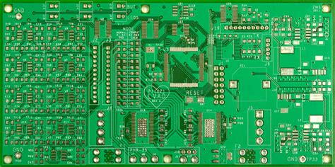
Key Functions of a Printed Circuit Board
PCBs serve several critical roles in electronic devices and systems:
- Providing a structural base for mounting components
- Electrically connecting components via conductive copper traces
- Insulating conductive pathways to prevent short circuits
- Dissipating heat generated by components during operation
- Shielding sensitive circuits from electromagnetic interference (EMI)
Structural Support for Electronic Components
One of the primary roles of a PCB is to provide a stable platform on which to mount and securely fasten electronic components. The rigid, non-conductive substrate material, typically FR4 fiberglass, acts as a durable base to physically support parts like integrated circuits, capacitors, resistors, and connectors soldered to the board. This ensures components remain in place despite any vibration, impact or mechanical stress the device may encounter.
Some of the common techniques used to attach components to a PCB include:
| Technique | Description |
|---|---|
| Through-hole mounting | Component leads are inserted into drilled holes and soldered to pads on the opposite side |
| Surface mount technology (SMT) | Components are soldered directly onto pads on the PCB surface without through-holes |
| Mixed technology | A combination of through-hole and SMT used on the same board |
Electrical Connectivity via Conductive Traces
The second key function of a PCB is to electrically interconnect the various components mounted on the board to create a functional circuit. This is achieved through conductive copper tracks, called traces, which are etched or printed onto the PCB substrate according to the specific circuit design.
These traces, along with other features like pads, vias and planes, create the conductive pathways that allow electrical signals and power to flow between components. The pattern of copper traces essentially forms the wiring diagram or schematic of the circuit.
Some important aspects of PCB trace design include:
-
Trace width: The width of a trace determines its current carrying capacity and resistance. Wider traces can handle higher currents and have lower resistance.
-
Trace spacing: Adequate spacing between traces is necessary to prevent unintended interactions, crosstalk or short circuits, especially for high-frequency signals.
-
Trace routing: The placement and path of traces should be optimized to minimize signal reflections, crosstalk and electromagnetic interference while keeping connections as short as possible.
Advanced PCBs often feature multiple copper layers, allowing for more complex interconnections and higher component density. Multi-layer boards have traces on both the top and bottom surfaces as well as inner layers sandwiched in the substrate.
| Number of Layers | Typical Applications |
|---|---|
| Single layer | Simple circuits, low-cost consumer electronics |
| Double layer | General purpose applications, moderate complexity |
| 4-8 layers | Complex digital systems, high-speed designs |
| 10+ layers | Highly complex devices, advanced computing, telecom |
Electrical Insulation and Isolation
In addition to providing conductive pathways, PCBs also serve the vital role of electrically insulating and isolating these conductive traces and components. The non-conductive substrate material, like FR4, prevents short circuits and unintended interactions between different parts of the circuit.
Some techniques used to enhance insulation and isolation on PCBs include:
-
Solder mask: A thin polymer coating applied over the copper traces, leaving only the pads and other features exposed for soldering. The solder mask protects the traces and prevents solder bridges or short circuits.
-
Isolation milling: Removing areas of copper to create separation between traces or components, especially for high-voltage applications.
-
Insulated metallic substrate (IMS): A special type of PCB with a thermally conductive dielectric layer to improve heat dissipation for power electronics while maintaining electrical insulation.
Proper insulation and isolation are critical to ensure the reliability, safety and performance of electronic circuits, particularly for high-voltage or high-frequency applications.
Heat Dissipation and Thermal Management
Electronic components generate heat during operation, which must be effectively dissipated to prevent damage, performance degradation or failure. PCBs play a key role in transferring this heat away from components and into the environment.
The copper traces and planes on a PCB not only provide electrical connectivity but also serve as thermal pathways to conduct heat away from components. The large surface area of copper planes, in particular, helps to spread heat more evenly across the board.
Some strategies used to enhance heat dissipation on PCBs include:
-
Thermal vias: Small holes drilled through the PCB and plated with copper to transfer heat from one side of the board to the other or into internal copper planes.
-
Heatsinks: Metal structures attached to components or the PCB to increase the surface area for heat dissipation into the surrounding air.
-
Metal core PCBs: Boards with a metal substrate, typically aluminum, that provides a direct thermal path to conduct heat away from components more efficiently than standard FR4.
Effective thermal management is crucial to ensure the long-term reliability and performance of electronic devices, especially for high-power applications or environments with limited airflow.
Shielding Sensitive Circuits from EMI
Electronic circuits, particularly those dealing with high-frequency signals or sensitive analog measurements, can be susceptible to electromagnetic interference (EMI) from external sources or other parts of the system. PCBs offer several ways to shield and protect sensitive circuits from EMI.
Some common PCB shielding techniques include:
-
Ground planes: Large areas of copper that provide a low-impedance return path for currents, helping to reduce EMI by minimizing loop areas.
-
Shielding cans: Metal enclosures soldered onto the PCB that completely surround sensitive components or circuits, blocking external EMI.
-
Trace routing: Careful placement and routing of traces to minimize loop areas, separate sensitive signals from potential sources of interference, and avoid coupling between traces.
-
Filtering: Incorporating filtering components like capacitors, ferrites or EMI filters on the PCB to suppress high-frequency noise and transients.
Effective EMI shielding and suppression techniques are essential for maintaining signal integrity, reducing crosstalk and ensuring reliable operation, especially in noisy environments or for applications with strict electromagnetic compatibility (EMC) requirements.
Frequently Asked Questions (FAQ)
1. What materials are PCBs typically made from?
PCBs are typically made from a composite material called FR4, which consists of woven fiberglass fabric impregnated with an epoxy resin. The copper conductive layers are laminated onto this FR4 substrate using heat and pressure. Other materials used in PCB fabrication include:
- Solder mask: A polymer coating applied over the copper traces for protection and insulation
- Silkscreen: A layer of ink used to print text, logos or component identifiers on the PCB surface
- Surface finishes: Coatings like HASL, ENIG or OSP applied to the exposed copper pads to prevent oxidation and enhance solderability
2. What are the differences between through-hole and surface mount PCB assembly?
Through-hole and surface mount are two different methods of attaching components to a PCB:
-
Through-hole mounting involves inserting component leads through drilled holes in the PCB and soldering them to pads on the opposite side. This method is older, simpler and generally more robust, but consumes more board space and limits component density.
-
Surface mount technology (SMT) involves soldering components directly onto pads on the surface of the PCB, without any through-holes. SMT allows for smaller components, higher density and faster automated assembly, but requires more precise manufacturing and can be more susceptible to mechanical stress.
Many modern PCBs use a mix of through-hole and SMT components to balance ease of assembly, reliability and component density.
3. How do vias work in a multi-layer PCB?
Vias are small holes drilled through a PCB and plated with conductive material, typically copper, to create electrical connections between different layers of the board. There are several types of vias:
- Through vias: Holes that go completely through the board from top to bottom, connecting all layers in between.
- Blind vias: Holes that start on an outer layer and terminate on an inner layer, without going through the entire board.
- Buried vias: Holes that connect inner layers without reaching either outer surface of the PCB.
Vias allow designers to create complex interconnections between components on different layers of a multi-layer PCB, enabling higher density and more efficient use of board space.
4. What is the role of solder mask on a PCB?
Solder mask is a thin polymer coating applied over the copper traces on a PCB, leaving only the pads and other features that need to be soldered exposed. The main functions of solder mask are:
- Insulation: Preventing short circuits and unintended connections between closely spaced traces.
- Protection: Guarding the copper traces against oxidation, corrosion and mechanical damage.
- Solder control: Limiting the flow of molten solder during assembly to prevent bridging between pads or components.
Solder mask also provides a cosmetic finish to the PCB and can be used to display text, logos or other markings on the board surface.
5. How do PCBs dissipate heat generated by components?
PCBs play a crucial role in transferring heat away from electronic components to prevent overheating and ensure reliable operation. Some ways PCBs facilitate heat dissipation include:
-
Copper traces and planes: The large surface area and high thermal conductivity of copper traces and planes help to spread heat more evenly across the board and into the environment.
-
Thermal vias: Small holes drilled through the PCB and plated with copper to conduct heat from one side of the board to the other or into internal copper planes.
-
Metal core substrates: PCBs with a metal base layer, typically aluminum, that provides a direct thermal path to efficiently transfer heat away from components.
-
Heatsinks and cooling solutions: Metal structures or other cooling devices attached to the PCB or individual components to increase the surface area for heat dissipation into the surrounding air.
Effective thermal management through careful PCB design and material selection is essential to ensure the long-term reliability and performance of electronic devices.
Conclusion
The main function of a PCB is to serve as a central platform for mechanically supporting and electrically interconnecting electronic components using conductive pathways. However, PCBs also play critical roles in insulating and isolating circuits, dissipating heat, and shielding sensitive components from electromagnetic interference.
By understanding the various functions and design aspects of PCBs, engineers and manufacturers can create more reliable, efficient, and high-performance electronic devices for a wide range of applications. As electronics continue to advance and become more complex, the importance of well-designed and manufactured PCBs will only continue to grow.

Leave a Reply