Introduction to Tenting Via in PCB Fabrication
Printed Circuit Board (PCB) fabrication is a complex process that involves various techniques and methods to create a functional and reliable electronic device. One of the crucial aspects of PCB fabrication is the use of vias, which are small holes drilled through the PCB to connect different layers of the board. Tenting via is a technique used in PCB fabrication to cover these vias with a thin layer of solder mask, providing additional protection and insulation to the board.
What is a Via?
A via is a small hole drilled through a PCB to connect different layers of the board. Vias are used to create electrical connections between different components on the PCB, allowing signals to pass through the board. There are several types of vias used in PCB fabrication, including:
- Through-hole vias: These are the most common type of vias, drilled through the entire thickness of the PCB.
- Blind vias: These vias are drilled from one side of the PCB and stop at a specific layer within the board.
- Buried vias: These vias are drilled between two inner layers of the PCB and are not visible from the surface.
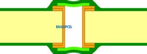
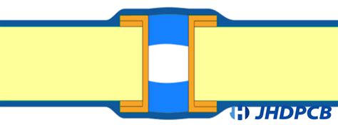
What is Tenting Via?
Tenting via is a technique used in PCB fabrication to cover the vias with a thin layer of solder mask. The solder mask is a protective coating applied to the surface of the PCB to prevent short circuits and provide insulation between the different components on the board. When a via is tented, the solder mask covers the entire via, including the hole and the surrounding area.
Advantages of Tenting Via
Tenting via provides several advantages in PCB fabrication, including:
-
Improved insulation: By covering the vias with solder mask, tenting via provides additional insulation between the different layers of the PCB, reducing the risk of short circuits and other electrical issues.
-
Enhanced protection: Tenting via helps protect the vias from physical damage, such as scratches or impacts, which can cause electrical failures in the PCB.
-
Reduced solder bridging: When vias are left exposed, there is a risk of solder bridging during the soldering process, which can cause short circuits and other issues. Tenting via helps prevent solder bridging by covering the vias with solder mask.
-
Improved manufacturability: Tenting via can help simplify the PCB fabrication process by reducing the need for additional steps, such as filling the vias with conductive material or applying additional insulation.
Disadvantages of Tenting Via
While tenting via provides several advantages in PCB fabrication, there are also some potential disadvantages to consider, including:
-
Increased cost: Tenting via requires additional solder mask material and processing steps, which can increase the overall cost of PCB fabrication.
-
Reduced thermal conductivity: When vias are tented, the solder mask material can act as a thermal insulator, reducing the ability of the PCB to dissipate heat. This can be a concern in high-power applications where thermal management is critical.
-
Potential for air pockets: If the solder mask material does not completely fill the via holes, air pockets can form, which can lead to reliability issues over time.
Tenting Via Techniques
There are several techniques used for tenting vias in PCB fabrication, each with its own advantages and disadvantages.
Full Tenting
Full tenting is a technique where the entire via, including the hole and surrounding area, is covered with solder mask material. This provides maximum insulation and protection for the via but can also increase the overall thickness of the PCB.
Partial Tenting
Partial tenting is a technique where only a portion of the via, typically the top and bottom surfaces, is covered with solder mask material. This can help reduce the overall thickness of the PCB while still providing some level of insulation and protection for the via.
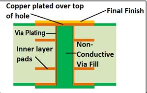
Plugged Vias
Plugged vias are a variation of tenting via where the via hole is filled with a non-conductive material, such as epoxy or resin, before being covered with solder mask. This provides additional insulation and protection for the via but can also increase the overall cost and complexity of the PCB fabrication process.
Tenting Via Design Considerations
When designing a PCB that will use tenting vias, there are several key considerations to keep in mind:
Via Size and Spacing
The size and spacing of the vias can have a significant impact on the effectiveness of tenting via. Smaller vias with tighter spacing may be more difficult to tent effectively, while larger vias with wider spacing may require more solder mask material and increase the overall thickness of the PCB.
Solder Mask Material
The choice of solder mask material can also impact the effectiveness of tenting via. Some solder mask materials may be more effective at filling via holes and providing insulation, while others may be more prone to air pockets or other defects.
Thermal Management
As mentioned earlier, tenting via can reduce the thermal conductivity of the PCB, which can be a concern in high-power applications. When designing a PCB with tented vias, it is important to consider the thermal management requirements of the application and choose materials and techniques that will provide adequate heat dissipation.

Tenting Via in Different PCB Applications
Tenting via is used in a wide range of PCB applications, from consumer electronics to aerospace and defense. Here are some examples of how tenting via is used in different industries:
Consumer Electronics
In consumer electronics, such as smartphones and laptops, tenting via is often used to provide additional insulation and protection for high-density PCBs with small vias and tight spacing. Tenting via can help prevent short circuits and other reliability issues in these devices.
Automotive Electronics
In automotive electronics, such as engine control modules and infotainment systems, tenting via is used to provide additional insulation and protection against the harsh environmental conditions that these devices may be exposed to, such as extreme temperatures, vibration, and moisture.
Medical Devices
In medical devices, such as implantable devices and diagnostic equipment, tenting via is used to provide additional insulation and protection against the biological fluids and tissues that these devices may come into contact with. Tenting via can help prevent corrosion and other reliability issues in these critical applications.
Aerospace and Defense
In aerospace and defense applications, such as satellites and military communications equipment, tenting via is used to provide additional insulation and protection against the extreme environmental conditions that these devices may be exposed to, such as radiation, vacuum, and extreme temperatures.
Frequently Asked Questions (FAQ)
-
What is the difference between tenting via and plugging via?
Tenting via involves covering the via with solder mask material, while plugging via involves filling the via hole with a non-conductive material before covering it with solder mask. Plugging via provides additional insulation and protection but can also increase the cost and complexity of the PCB fabrication process. -
Can tenting via be used on both sides of the PCB?
Yes, tenting via can be used on both sides of the PCB, depending on the design requirements and the PCB fabrication process being used. -
How does tenting via impact the cost of PCB fabrication?
Tenting via typically increases the cost of PCB fabrication, as it requires additional solder mask material and processing steps. However, the cost impact may vary depending on the specific design requirements and the PCB fabrication process being used. -
Can tenting via be used with all types of vias?
Tenting via can be used with most types of vias, including through-hole, blind, and buried vias. However, the effectiveness of tenting via may vary depending on the size and spacing of the vias, as well as the solder mask material being used. -
What are some of the key design considerations when using tenting via?
Some of the key design considerations when using tenting via include via size and spacing, solder mask material selection, and thermal management requirements. It is important to carefully consider these factors to ensure the effectiveness and reliability of the tented vias in the final PCB assembly.
| Tenting Via Technique | Advantages | Disadvantages |
|---|---|---|
| Full Tenting | Maximum insulation and protection for the via | Increases overall thickness of the PCB |
| Partial Tenting | Reduces overall thickness of the PCB while still providing some insulation and protection for the via | May not provide as much insulation and protection as full tenting |
| Plugged Vias | Provides additional insulation and protection for the via | Increases cost and complexity of the PCB fabrication process |
Conclusion
Tenting via is a crucial technique used in PCB fabrication to provide additional insulation, protection, and reliability for the vias that connect different layers of the board. By covering the vias with solder mask material, tenting via helps prevent short circuits, reduce solder bridging, and improve the overall manufacturability of the PCB.
When designing a PCB that will use tenting vias, it is important to carefully consider factors such as via size and spacing, solder mask material selection, and thermal management requirements to ensure the effectiveness and reliability of the tented vias in the final PCB assembly.
Tenting via is used in a wide range of PCB applications, from consumer electronics to aerospace and defense, and provides critical protection and insulation for these devices in often harsh and demanding environments.
As PCB technology continues to advance and the demand for high-density, high-reliability electronic devices grows, tenting via will likely remain an essential technique in PCB fabrication for the foreseeable future.
Leave a Reply