Introduction to Single-Layer PCB
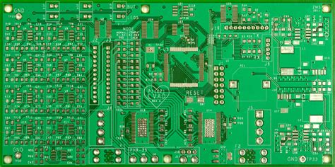
A Single-Layer PCB, also known as a single-sided PCB, is a printed circuit board that has only one layer of conductive material, typically copper, on one side of the insulating substrate. This layer is used for both signal traces and component pads. Single-Layer PCBs are the simplest and most cost-effective type of PCB, making them ideal for basic electronic projects and low-complexity circuits.
Advantages of Single-Layer PCBs
- Cost-effective: Single-Layer PCBs are the most affordable type of PCB due to their simple design and manufacturing process.
- Easy to design: With only one conductive layer, Single-Layer PCBs are easier to design compared to multi-layer PCBs.
- Quick turnaround: The manufacturing process for Single-Layer PCBs is faster than that of multi-layer PCBs, resulting in shorter lead times.
- Suitable for low-complexity circuits: Single-Layer PCBs are ideal for simple electronic projects and low-complexity circuits.
Disadvantages of Single-Layer PCBs
- Limited routing options: With only one conductive layer, Single-Layer PCBs have limited routing options, which can make it challenging to design complex circuits.
- Lower component density: Due to the limited routing options, Single-Layer PCBs typically have lower component density compared to multi-layer PCBs.
- Reduced electrical performance: Single-Layer PCBs may have reduced electrical performance compared to multi-layer PCBs, particularly in high-frequency applications.
Manufacturing Process of Single-Layer PCBs
The manufacturing process of Single-Layer PCBs involves several steps:
- Design: The PCB design is created using CAD software, which generates the necessary files for manufacturing.
- Copper cladding: A thin layer of copper is bonded to one side of the insulating substrate, typically FR-4.
- Printing: The PCB design is printed onto the copper layer using a photoresist material.
- Etching: The unwanted copper is removed using a chemical etching process, leaving only the desired traces and pads.
- Drilling: Holes are drilled through the PCB for component leads and vias.
- Silkscreen and solder mask: A silkscreen layer is applied for component labels and a solder mask is added to protect the copper traces.
- Surface finish: A surface finish, such as HASL or ENIG, is applied to the exposed copper to improve solderability and protect against oxidation.

Design Considerations for Single-Layer PCBs
When designing Single-Layer PCBs, there are several factors to consider:
- Trace width and spacing: Ensure that the trace width and spacing are appropriate for the current and voltage requirements of the circuit.
- Component placement: Optimize component placement to minimize trace lengths and reduce signal interference.
- Grounding: Provide adequate grounding to minimize noise and ensure proper circuit functionality.
- Vias: Use vias sparingly, as they can add complexity to the manufacturing process and increase costs.
- Routing: Carefully plan the routing to avoid signal interference and minimize trace lengths.

Applications of Single-Layer PCBs
Single-Layer PCBs are used in a variety of applications, including:
- Simple electronic projects: Single-Layer PCBs are ideal for basic electronic projects, such as LED circuits, simple amplifiers, and power supplies.
- Low-complexity circuits: Single-Layer PCBs are suitable for low-complexity circuits, such as sensors, switches, and simple control systems.
- Prototyping: Single-Layer PCBs are often used for prototyping and testing new designs before moving to more complex multi-layer PCBs.
- Educational purposes: Single-Layer PCBs are commonly used in educational settings to teach basic electronics and PCB design principles.

Comparison of Single-Layer PCBs and Multi-Layer PCBs
| Feature | Single-Layer PCB | Multi-Layer PCB |
|---|---|---|
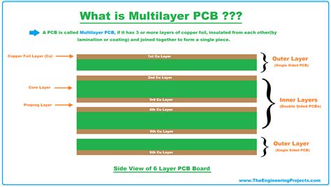
| Conductive layers | 1 | 2 or more |
| Cost | Low | High |
| Design complexity | Low | High |
| Component density | Low | High |
| Electrical performance | Low to moderate | High |
| Manufacturing time | Fast | Slow |
| Applications | Simple circuits | Complex circuits |
FAQ
1. What is the typical thickness of a Single-Layer PCB?
The typical thickness of a Single-Layer PCB is 1.6 mm (0.063 inches), although thinner and thicker options are available depending on the application and manufacturing capabilities.
2. Can Single-Layer PCBs have components on both sides?
Yes, Single-Layer PCBs can have components on both sides, but the routing is limited to one side of the board. This is known as a single-sided assembly.
3. What is the maximum number of components that can be placed on a Single-Layer PCB?
The maximum number of components that can be placed on a Single-Layer PCB depends on various factors, such as the size of the board, the size of the components, and the complexity of the routing. Generally, Single-Layer PCBs have lower component density compared to multi-layer PCBs.
4. Are Single-Layer PCBs suitable for high-frequency applications?
Single-Layer PCBs may not be the best choice for high-frequency applications due to their limited routing options and potential for signal interference. In such cases, multi-layer PCBs with dedicated power and ground planes are often preferred.
5. Can Single-Layer PCBs be used for mass production?
Yes, Single-Layer PCBs can be used for mass production, particularly for simple and low-cost electronic products. However, for more complex designs and higher production volumes, multi-layer PCBs may be more cost-effective in the long run.
Conclusion
Single-Layer PCBs are a simple, cost-effective solution for basic electronic projects and low-complexity circuits. While they have limitations in terms of routing options and component density, they offer several advantages, such as quick turnaround times and easy design processes. When deciding between Single-Layer and multi-layer PCBs, it is essential to consider the specific requirements of the application, including the complexity of the circuit, electrical performance needs, and production volume. By understanding the characteristics and manufacturing process of Single-Layer PCBs, designers can make informed decisions and create successful electronic products.

Leave a Reply