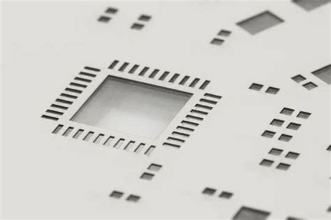
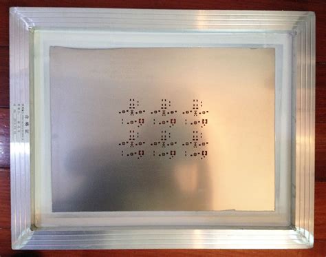
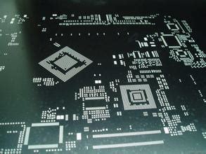
The Role of PCB Stencils in SMT Assembly
PCB stencils play a crucial role in the SMT assembly process, which involves placing surface mount devices (SMDs) onto the pads of a PCB and securing them in place with solder. The key steps in the SMT assembly process where PCB stencils are used include:
-
Solder Paste Application: The PCB stencil is aligned with the PCB, and solder paste is applied to the stencil’s surface. A squeegee is then used to spread the paste across the stencil, forcing it through the openings and onto the PCB pads.
-
Component Placement: After the solder paste is applied, SMDs are placed onto the PCB pads, either manually or using an automated pick-and-place machine.
-
Reflow Soldering: The PCB with the placed components is then subjected to a reflow soldering process, where the board is heated to melt the solder paste, forming a permanent electrical and mechanical connection between the components and the PCB pads.
PCB stencils ensure that the correct amount of solder paste is applied to each pad, which is essential for creating reliable solder joints and preventing defects such as bridging, insufficient solder, or tombstoning.
Types of PCB Stencils
There are several types of PCB stencils available, each with its own advantages and disadvantages. The most common types include:
Stainless Steel Stencils
Stainless steel stencils are the most widely used type of PCB stencil due to their durability, precision, and long lifespan. They are typically laser-cut from thin sheets of stainless steel, with thicknesses ranging from 0.1 mm to 0.2 mm (4 to 8 mils). Stainless steel stencils can be used for high-volume production and are suitable for a wide range of solder paste types and PCB designs.
Polyimide Stencils
Polyimide stencils, also known as polymer stencils, are made from a flexible, heat-resistant plastic material. They are laser-cut and offer several advantages over stainless steel stencils, such as lower cost, improved flexibility, and better conformity to uneven PCB surfaces. However, polyimide stencils have a shorter lifespan and are less durable than stainless steel stencils, making them more suitable for low-volume production or prototyping.
Nickel Stencils
Nickel stencils are electroformed from a thin layer of nickel and offer high precision and durability. They are particularly useful for fine-pitch applications and designs with very small apertures. Nickel stencils have a smooth surface finish that helps prevent solder paste from sticking to the stencil, improving the transfer efficiency and reducing the need for frequent cleaning.
Frameless Stencils
Frameless stencils, also known as foil stencils, are made from a thin sheet of stainless steel or polyimide without a rigid frame. They are designed to be used with a dedicated stencil holder or frame system, allowing for quick and easy changeovers between different stencil designs. Frameless stencils are more cost-effective and take up less storage space compared to framed stencils.

Factors Affecting PCB Stencil Performance
Several factors can impact the performance of a PCB stencil and the quality of the solder paste deposition. These include:
Stencil Thickness
The thickness of a PCB stencil determines the amount of solder paste deposited onto the PCB pads. Thicker stencils deposit more paste, while thinner stencils deposit less. The optimal stencil thickness depends on the size and pitch of the components, the PCB design, and the solder paste type. Common stencil thicknesses range from 0.1 mm to 0.2 mm (4 to 8 mils).
Aperture Design
The design of the stencil apertures, including their size, shape, and orientation, affects the solder paste release and the resulting solder joint quality. Apertures that are too small or have an inappropriate shape can lead to insufficient solder paste deposition or inconsistent release. Aperture design guidelines, such as the aspect ratio (width to thickness) and area ratio (aperture area to wall area), should be followed to ensure optimal solder paste release.
Stencil Material
The choice of stencil material impacts its durability, precision, and compatibility with different solder paste types. Stainless steel stencils are the most common and offer high durability and precision, while polyimide stencils are more flexible and conformable but have a shorter lifespan. Nickel stencils provide excellent surface finish and are suitable for fine-pitch applications.
Stencil Coating
Stencil coatings, such as nano-coating or PTFE (polytetrafluoroethylene) coating, can be applied to the surface of the stencil to improve its performance. These coatings help prevent solder paste from sticking to the stencil, enhance the paste release, and reduce the need for frequent cleaning. Coated stencils can improve print quality, increase stencil lifespan, and reduce maintenance requirements.

PCB Stencil Design Guidelines
To ensure optimal solder paste deposition and high-quality solder joints, follow these PCB stencil design guidelines:
-
Aperture Size: The aperture size should be slightly larger than the PCB pad size to accommodate the solder paste volume and allow for some misalignment. A common rule of thumb is to add 10% to 20% to the pad size when designing the aperture.
-
Aperture Shape: The aperture shape should match the shape of the PCB pad, such as rectangular for SMD pads and circular for through-hole pads. For fine-pitch components or small apertures, tapered or rounded aperture walls can improve solder paste release.
-
Aspect Ratio: The aspect ratio, which is the ratio of the aperture width to the stencil thickness, should be between 1.5 and 2.0 for optimal solder paste release. Apertures with aspect ratios below 1.5 may result in insufficient paste release, while aspect ratios above 2.0 may lead to excessive paste deposition.
-
Area Ratio: The area ratio, which is the ratio of the aperture area to the aperture wall area, should be greater than 0.66 for reliable solder paste release. Lower area ratios can result in poor paste release and inconsistent deposition.
-
Stencil Thickness: Choose the appropriate stencil thickness based on the component size, pitch, and solder paste volume requirements. Thicker stencils (0.15 mm to 0.2 mm) are suitable for larger components and higher volume deposits, while thinner stencils (0.1 mm to 0.15 mm) are better for smaller components and finer pitches.
-
Fiducial Marks: Include fiducial marks on the stencil to aid in alignment with the PCB. Fiducial marks should be located near the corners of the stencil and have a unique shape or pattern to ensure accurate recognition by vision systems.
-
Stencil Frame: For framed stencils, choose a frame size and mounting method compatible with your solder paste printer or stencil holder. Ensure that the frame is sturdy and provides adequate support to prevent stencil warping or damage.

PCB Stencil Maintenance and Cleaning
Proper maintenance and cleaning of PCB stencils are essential for ensuring consistent solder paste deposition and high-quality prints. Follow these best practices:
-
Regular Inspection: Inspect the stencil regularly for signs of wear, damage, or clogging. Check for bent or damaged apertures, solder paste buildup, or other irregularities that may affect print quality.
-
Cleaning Frequency: Clean the stencil after every print cycle or as needed based on the solder paste type and volume of production. More frequent cleaning may be necessary for high-volume production or when using no-clean solder pastes.
-
Cleaning Methods: Use appropriate cleaning methods and solutions based on the stencil material and solder paste type. Common cleaning methods include manual wiping with isopropyl alcohol (IPA), ultrasonic cleaning, and automated stencil cleaning systems.
-
Stencil Storage: Store the stencil in a clean, dry environment to prevent damage or contamination. Use a stencil storage rack or cabinet to keep the stencil flat and protected from dust or debris.
-
Handling and Transport: Handle the stencil with care to avoid bending, warping, or damaging the apertures. Use a stencil handling frame or carrier when transporting the stencil between the storage area and the solder paste printer.
By following proper maintenance and cleaning procedures, you can extend the lifespan of your PCB stencils and ensure consistent, high-quality solder paste prints.
Frequently Asked Questions (FAQ)
1. What is the difference between a PCB stencil and a solder paste mask?
A PCB stencil is a separate sheet of material with openings that correspond to the pads on a PCB, used to apply solder paste during the SMT assembly process. A solder paste mask, on the other hand, is a layer of the PCB itself that defines the areas where solder paste should be applied. The solder paste mask is typically created during the PCB fabrication process and is an integral part of the board.
2. Can PCB stencils be reused?
Yes, PCB stencils can be reused multiple times with proper cleaning and maintenance. Stainless steel stencils have the longest lifespan and can be used for thousands of print cycles, while polyimide stencils have a shorter lifespan and may need to be replaced more frequently.
3. How do I choose the right stencil thickness for my PCB?
The optimal stencil thickness depends on several factors, including the component size, pitch, and solder paste volume requirements. As a general guideline, use thicker stencils (0.15 mm to 0.2 mm) for larger components and higher volume deposits, and thinner stencils (0.1 mm to 0.15 mm) for smaller components and finer pitches. Consult with your stencil manufacturer or solder paste supplier for specific recommendations based on your PCB design.
4. What is the purpose of fiducial marks on a PCB stencil?
Fiducial marks on a PCB stencil serve as reference points for aligning the stencil with the PCB during the solder paste printing process. They help ensure accurate and consistent alignment, minimizing the risk of solder paste offset or misregistration. Fiducial marks should have a unique shape or pattern and be located near the corners of the stencil for easy recognition by vision systems.
5. How often should I clean my PCB stencil?
The frequency of PCB stencil cleaning depends on several factors, such as the solder paste type, volume of production, and environmental conditions. As a general rule, clean the stencil after every print cycle or as needed based on the observed print quality. More frequent cleaning may be necessary for high-volume production or when using no-clean solder pastes that tend to dry and accumulate on the stencil surface. Regular inspection and cleaning help maintain consistent solder paste deposition and prevent defects caused by clogged or contaminated apertures.
Conclusion
PCB stencils are essential tools in the SMT assembly process, ensuring precise and consistent solder paste deposition onto PCB pads. By selecting the appropriate stencil type, material, and thickness, and following proper design guidelines and maintenance practices, you can achieve high-quality solder joints and reliable PCB assemblies. Understanding the role of PCB stencils and their impact on the solder paste printing process is crucial for optimizing your SMT assembly workflow and minimizing defects.
As technology advances and component sizes continue to shrink, the importance of PCB stencils in achieving accurate and reliable solder paste deposition will only increase. Staying up-to-date with the latest stencil technologies, design guidelines, and best practices will help you stay competitive in the ever-evolving world of PCB assembly.

Leave a Reply