Understanding PCB Projects
What is a PCB?
A PCB is a flat board made of insulating material, such as fiberglass or plastic, with conductive tracks etched on its surface. These tracks connect various electronic components, such as resistors, capacitors, and integrated circuits, to form a complete electronic circuit. PCBs provide a stable and reliable platform for electronic circuits, making them essential in modern electronics.
Types of PCB Projects
PCB projects can be categorized based on their complexity and application:
-
Hobby Projects: These are small-scale projects often undertaken by electronics enthusiasts for learning or personal use. Examples include LED displays, simple robots, and DIY audio amplifiers.
-
Educational Projects: PCB projects are frequently used in educational settings to teach students about electronics, circuit design, and programming. These projects help students gain hands-on experience and develop practical skills.
-
Commercial Projects: Many businesses rely on custom PCB designs for their products or services. These projects often involve more complex circuits and require higher levels of reliability and performance.
-
Industrial Projects: PCBs are widely used in industrial applications, such as control systems, monitoring devices, and automation equipment. These projects often have stringent requirements for durability, safety, and environmental resistance.
Benefits of PCB Projects
PCB projects offer several advantages over traditional breadboard or point-to-point wiring:
-
Reliability: PCBs provide a stable and reliable platform for electronic circuits, reducing the risk of loose connections or short circuits.
-
Compact Size: PCBs allow for miniaturization of electronic devices, making them suitable for portable and space-constrained applications.
-
Ease of Replication: Once a PCB design is finalized, it can be easily replicated, making mass production more efficient and cost-effective.
-
Improved Signal Integrity: PCBs can be designed with controlled impedance and proper grounding, ensuring better signal integrity and reducing electromagnetic interference (EMI).
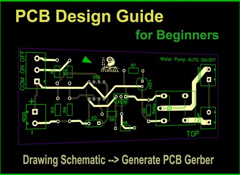
The PCB Project Workflow
The process of creating a PCB project involves several stages:
1. Circuit Design
The first step in any PCB project is to design the electronic circuit. This involves selecting the appropriate components, determining their values, and creating a schematic diagram. Various software tools, such as EDA (Electronic Design Automation) software, are used for this purpose.
2. PCB Layout
Once the circuit design is finalized, the next step is to create the PCB layout. This involves arranging the components on the PCB and routing the conductive tracks to connect them. PCB layout software is used to create the layout, ensuring proper spacing, trace width, and other design rules are followed.
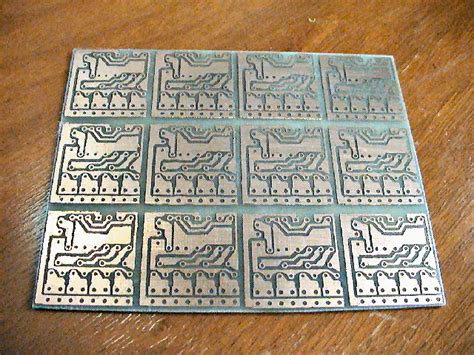
3. PCB Fabrication
After the PCB layout is complete, the design files are sent to a PCB fabrication house. The fabrication process involves several steps, such as:
- Printing the circuit pattern on the copper-clad board
- Etching away the unwanted copper
- Drilling holes for through-hole components
- Applying solder mask and silkscreen
The fabricated PCBs are then tested for quality and functionality.
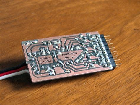
4. PCB Assembly
The final step in a PCB project is to assemble the components onto the fabricated PCB. This can be done manually for small-scale projects or using automated pick-and-place machines for larger production runs. After assembly, the PCB is tested and debugged to ensure proper functionality.
Tools and Resources for PCB Projects
Several tools and resources are available to help with PCB projects:
EDA Software
EDA software is used for circuit design and simulation. Popular options include:
| Software | Description |
|---|---|
| KiCad | A free and open-source EDA suite for schematic capture and PCB layout |
| Eagle | A widely used EDA tool with a large component library and active community |
| Altium Designer | A professional-grade EDA software with advanced features and collaboration tools |
PCB Fabrication Services
Many online PCB fabrication services offer affordable and quick turnaround for prototype and small-batch PCBs. Some popular options include:
| Service | Description |
|---|---|
| JLCPCB | A low-cost PCB fabrication service with a user-friendly ordering process |
| PCBWay | Offers a wide range of PCB fabrication options, including flexible and rigid-flex PCBs |
| OSH Park | A community-driven PCB fabrication service with a unique purple soldermask |
Online Communities and Resources
There are numerous online communities and resources dedicated to PCB projects and electronics:
| Resource | Description |
|---|---|
| Arduino Forum | A large community of Arduino enthusiasts sharing projects, tutorials, and troubleshooting tips |
| EEVblog Forum | An active forum for electronics engineers and hobbyists, covering various topics related to PCB design and fabrication |
| Hackaday | A popular blog featuring innovative electronics projects, tutorials, and news |
| Instructables | A platform for sharing DIY projects, including many electronics and PCB-related tutorials |

FAQ
-
What skills do I need to start a PCB project?
To start a PCB project, you should have a basic understanding of electronics, circuit design, and programming. Familiarity with EDA software and PCB layout principles is also helpful. -
How much does it cost to fabricate a PCB?
The cost of PCB fabrication depends on various factors, such as the board size, layer count, and quantity. For small prototype runs, the cost can range from a few dollars to a few hundred dollars. -
Can I make a PCB at home?
Yes, it is possible to make PCBs at home using various methods, such as toner transfer or photoresist etching. However, these methods often have limitations in terms of quality and complexity compared to professional fabrication services. -
How long does it take to complete a PCB project?
The time required to complete a PCB project depends on the complexity of the circuit, the experience of the designer, and the fabrication and assembly process. Simple projects can be completed in a few days, while more complex projects may take several weeks or months. -
What are some common mistakes to avoid in PCB projects?
Some common mistakes to avoid in PCB projects include: - Not properly checking the schematic for errors before proceeding to PCB layout
- Violating design rules, such as minimum trace width or clearance
- Not considering manufacturability and assembly requirements during the design phase
- Inadequate testing and debugging after assembly
Conclusion
PCB projects are an essential part of modern electronics, enabling the creation of reliable, compact, and efficient electronic devices. By understanding the PCB project workflow, utilizing the right tools and resources, and following best practices, anyone can embark on the exciting journey of creating custom PCBs. Whether you are a hobbyist, student, or professional, PCB projects offer endless opportunities for learning, innovation, and creativity in the world of electronics.
Leave a Reply