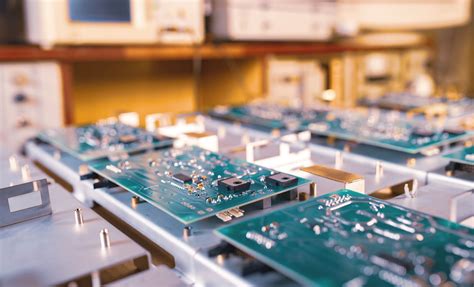
The Importance of PCB Manufacturing
PCB manufacturing plays a crucial role in the electronics industry, as it enables the production of complex electronic devices in a compact and efficient manner. Some of the key benefits of PCB manufacturing include:
-
Miniaturization: PCBs allow for the integration of multiple electronic components into a small, compact board, enabling the creation of smaller and more portable devices.
-
Reliability: Well-designed and manufactured PCBs ensure reliable connections between components, reducing the risk of electronic failures and improving the overall performance of the device.
-
Cost-effectiveness: PCB manufacturing enables mass production of electronic devices, reducing the cost per unit and making electronics more affordable for consumers.
-
Flexibility: PCBs can be designed and manufactured to suit a wide range of applications, from simple single-layer boards to complex multi-layer boards with advanced features.
The PCB Manufacturing Process
The PCB manufacturing process involves several key steps, each of which is crucial to ensuring the quality and reliability of the final product. These steps include:
1. PCB Design
The first step in PCB manufacturing is designing the circuit layout. This involves creating a schematic diagram of the electronic circuit, which shows the connections between the various components. The schematic is then used to create a PCB layout, which determines the placement of components and the routing of the copper traces that connect them.
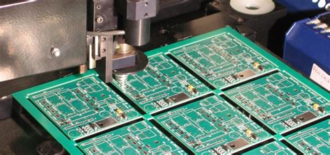
2. PCB Fabrication
Once the PCB layout is finalized, the next step is to fabricate the board. This involves several sub-steps, including:
-
Printing the circuit pattern: The PCB layout is printed onto a copper-clad laminate sheet using a photoresist process. The areas of the copper that will form the circuit traces are left exposed, while the rest of the copper is covered with the photoresist.
-
Etching: The exposed copper is then etched away using a chemical solution, leaving only the circuit traces behind.
-
Drilling: Holes are drilled into the board to accommodate through-hole components and to create vias, which are used to connect traces on different layers of the board.
-
Plating: The holes and vias are then plated with copper to ensure reliable electrical connections.
-
Applying solder mask: A solder mask is applied to the board to protect the copper traces from oxidation and to prevent solder bridges from forming between adjacent traces during the soldering process.
-
Applying silkscreen: Finally, a silkscreen layer is applied to the board, which includes text and symbols that help identify the components and their locations on the board.
3. PCB Assembly
After the PCB is fabricated, the next step is to assemble the electronic components onto the board. This involves several sub-steps, including:
-
Solder paste application: Solder paste is applied to the pads on the PCB where the components will be placed.
-
Component placement: The components are then placed onto the board using automated pick-and-place machines or by hand.
-
Reflow soldering: The board is then heated in a reflow oven, which melts the solder paste and creates a permanent electrical and mechanical connection between the components and the board.
-
Inspection and testing: Finally, the assembled PCB is inspected and tested to ensure that all the connections are correct and that the board is functioning as intended.
Types of PCBs
There are several types of PCBs, each with its own unique features and applications. Some of the most common types of PCBs include:
1. Single-Layer PCBs
Single-layer PCBs have copper traces on only one side of the board. They are the simplest and most cost-effective type of PCB, making them suitable for basic electronic projects and low-density circuits.
2. Double-Layer PCBs
Double-layer PCBs have copper traces on both sides of the board, allowing for more complex circuits and higher component density. They are commonly used in a wide range of electronic devices, from consumer electronics to industrial equipment.
3. Multi-Layer PCBs
Multi-layer PCBs have three or more layers of copper traces, separated by insulating layers. They are used in high-density, complex electronic devices that require a large number of interconnections, such as smartphones, computers, and medical equipment.
4. Flexible PCBs
Flexible PCBs are made from flexible materials, such as polyimide or PEEK, allowing them to bend and twist without damaging the circuit. They are commonly used in applications where the PCB needs to fit into a confined space or where the device is subject to frequent movement, such as in wearable electronics and automotive applications.
5. Rigid-Flex PCBs
Rigid-flex PCBs combine the benefits of both rigid and flexible PCBs, with rigid sections for mounting components and flexible sections for connecting them. They are used in applications where the PCB needs to be folded or bent to fit into a specific shape, such as in aerospace and military equipment.

PCB Manufacturing Materials
PCBs are made from a variety of materials, each with its own unique properties and characteristics. Some of the most common PCB materials include:
1. FR-4
FR-4 is the most widely used PCB material, consisting of a woven fiberglass cloth impregnated with an epoxy resin. It has excellent mechanical and electrical properties, making it suitable for a wide range of applications.
2. Polyimide
Polyimide is a high-performance polymer that is commonly used in flexible PCBs. It has excellent thermal and chemical resistance, as well as good mechanical and electrical properties.
3. PTFE
PTFE (polytetrafluoroethylene) is a fluoropolymer that is commonly used in high-frequency and microwave applications. It has a low dielectric constant and low loss tangent, making it ideal for high-speed signal transmission.
4. Aluminum
Aluminum PCBs are used in applications where heat dissipation is a critical factor, such as in power electronics and LED lighting. The aluminum substrate helps to quickly dissipate heat away from the components, improving the overall reliability and performance of the device.
PCB Design Considerations
Designing a PCB involves several key considerations to ensure optimal performance, reliability, and manufacturability. Some of the most important PCB design considerations include:
1. Component Placement
Components should be placed on the PCB in a way that minimizes the length of the interconnections and reduces the risk of signal interference. Critical components, such as high-speed devices and sensitive analog circuits, should be placed away from sources of noise and interference.
2. Signal Integrity
Signal integrity refers to the quality of the electrical signals transmitted through the PCB. To ensure good signal integrity, designers must carefully consider factors such as trace width, spacing, and impedance matching. High-speed signals may require specialized design techniques, such as controlled impedance routing and differential pair routing.
3. Power Distribution
Power distribution is another critical factor in PCB design. The PCB must be designed to provide a stable and reliable power supply to all the components, while minimizing voltage drop and power loss. This may involve the use of dedicated power planes, decoupling capacitors, and other power management techniques.
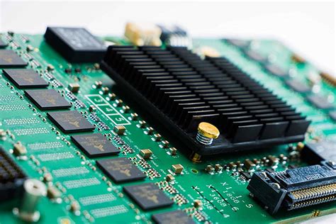
4. Thermal Management
Thermal management is essential to ensure that the components on the PCB operate within their specified temperature range. This may involve the use of thermal vias, heatsinks, and other cooling techniques to dissipate heat away from the components.
5. Manufacturing Considerations
Finally, PCB designers must consider the manufacturing process when designing the board. This includes factors such as minimum trace width and spacing, hole sizes, and solder mask clearances. Designers must also ensure that the PCB is compatible with the manufacturing equipment and processes used by the PCB fabricator.
PCB Manufacturing Standards
PCB manufacturing is governed by a set of industry standards that ensure consistency and reliability in the manufacturing process. Some of the most important PCB manufacturing standards include:
1. IPC Standards
The IPC (Institute of Printed Circuits) is a global trade association that develops and maintains standards for the electronics industry. Some of the most relevant IPC standards for PCB manufacturing include:
- IPC-2221: Generic Standard on Printed Board Design
- IPC-6012: Qualification and Performance Specification for Rigid Printed Boards
- IPC-A-600: Acceptability of Printed Boards
2. UL Standards
UL (Underwriters Laboratories) is a global safety certification company that develops standards for the safety and performance of electronic products. Some of the most relevant UL standards for PCB manufacturing include:
- UL 94: Standard for Safety of Flammability of Plastic Materials for Parts in Devices and Appliances
- UL 796: Standard for Safety of Printed-Wiring Boards
3. JEDEC Standards
JEDEC (Joint Electron Device Engineering Council) is a global standards organization that develops standards for the microelectronics industry. Some of the most relevant JEDEC standards for PCB manufacturing include:
- JESD22: Reliability Test Methods for Packaged Devices
- JESD625: Requirements for Handling Electrostatic-Discharge-Sensitive (ESDS) Devices
PCB Manufacturing Quality Control
Quality control is a critical aspect of PCB manufacturing, ensuring that the final product meets the required specifications and performs reliably in the intended application. Some of the key quality control measures in PCB manufacturing include:
1. Visual Inspection
Visual inspection is the first line of defense in PCB quality control, involving a visual examination of the board for defects such as missing or damaged components, solder bridges, and incorrect component placement.
2. Automated Optical Inspection (AOI)
AOI uses automated cameras and image processing software to inspect the PCB for defects that may be difficult to detect visually, such as small solder bridges or missing solder joints.
3. X-Ray Inspection
X-ray inspection is used to detect defects that are not visible on the surface of the PCB, such as voids in the solder joints or misaligned components.
4. Electrical Testing
Electrical testing involves applying electrical signals to the PCB and measuring the response to ensure that the board is functioning as intended. This may include continuity testing, insulation resistance testing, and functional testing.
Conclusion
PCB manufacturing is a complex and multifaceted process that involves several key steps, from designing the circuit layout to the final assembly of components onto the board. By understanding the different types of PCBs, materials, design considerations, and manufacturing standards involved in PCB manufacturing, engineers and manufacturers can ensure the production of high-quality, reliable electronic devices that meet the needs of a wide range of applications.
Frequently Asked Questions (FAQ)
- What is the difference between a single-layer and a double-layer PCB?
-
A single-layer PCB has copper traces on only one side of the board, while a double-layer PCB has copper traces on both sides of the board. Double-layer PCBs allow for more complex circuits and higher component density compared to single-layer PCBs.
-
What is the purpose of a solder mask in PCB manufacturing?
-
A solder mask is a protective layer applied to the PCB to protect the copper traces from oxidation and to prevent solder bridges from forming between adjacent traces during the soldering process.
-
What is the difference between a rigid and a flexible PCB?
-
A rigid PCB is made from a rigid material, such as FR-4, and is designed to maintain its shape and structure. A flexible PCB, on the other hand, is made from a flexible material, such as polyimide, and can bend and twist without damaging the circuit.
-
What is the role of IPC standards in PCB manufacturing?
-
IPC standards are industry-wide guidelines that ensure consistency and reliability in PCB manufacturing. They cover various aspects of PCB design, fabrication, and assembly, and help to ensure that PCBs meet the required quality and performance standards.
-
What are some of the key quality control measures used in PCB manufacturing?
- Some of the key quality control measures used in PCB manufacturing include visual inspection, automated optical inspection (AOI), X-ray inspection, and electrical testing. These measures help to identify and correct defects in the PCB, ensuring that the final product meets the required specifications and performs reliably in the intended application.
| PCB Type | Layers | Typical Applications |
|---|---|---|
| Single-layer PCB | 1 | Simple, low-density circuits |
| Double-layer PCB | 2 | Consumer electronics, industrial equipment |
| Multi-layer PCB | 3+ | High-density, complex devices (e.g., smartphones, computers) |
| Flexible PCB | Varies | Wearable electronics, automotive applications |
| Rigid-flex PCB | Varies | Aerospace, military equipment |
Leave a Reply