Understanding PCB Quality
Printed Circuit boards (PCBs) are the backbone of modern electronic devices. They provide the necessary interconnections between various components and ensure the proper functioning of the device. The quality of a PCB directly impacts the reliability, performance, and longevity of the electronic product. In this article, we will delve into the world of PCB quality and explore its various aspects.
What is a PCB?
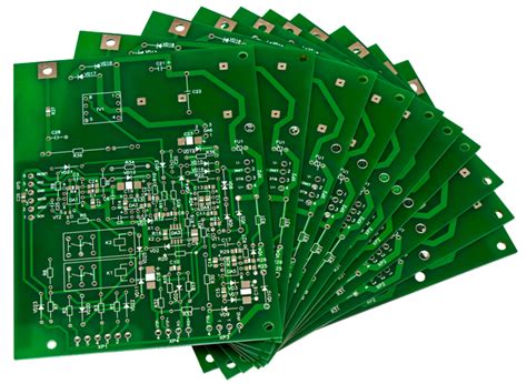
A Printed Circuit Board (PCB) is a flat board made of insulating materials, such as fiberglass or composite epoxy, with conductive copper tracks printed on its surface. These copper tracks form the electrical connections between different components mounted on the board. PCBs can be single-sided, double-sided, or multi-layered, depending on the complexity of the circuit and the space constraints.
Importance of PCB Quality
The quality of a PCB is crucial for several reasons:
-
Reliability: A high-quality PCB ensures reliable operation of the electronic device. It minimizes the risk of short circuits, open circuits, and other defects that can lead to device failure.
-
Performance: The quality of the PCB directly affects the performance of the electronic device. A well-designed and manufactured PCB ensures optimal signal integrity, minimizes electromagnetic interference (EMI), and enables the device to operate at its intended speed and efficiency.
-
Longevity: A high-quality PCB is more resistant to environmental factors such as temperature, humidity, and vibration. This increased durability translates to a longer lifespan for the electronic device.
-
Cost-effectiveness: Investing in high-quality PCBs reduces the likelihood of device failures and subsequent repair or replacement costs. It also minimizes the risk of product recalls and the associated financial and reputational damage.
Factors Affecting PCB Quality
Several factors contribute to the overall quality of a PCB. Let’s explore some of the key factors:
Design
The design of a PCB is the first and most critical step in ensuring its quality. A well-designed PCB takes into account various factors such as:
- Component placement: The placement of components on the PCB should be optimized for signal integrity, thermal management, and manufacturability.
- Trace routing: The copper traces should be designed to minimize signal reflections, crosstalk, and electromagnetic interference.
- Impedance control: The impedance of the traces should be carefully controlled to ensure proper signal transmission and minimize signal distortion.
- Thermal management: The PCB design should consider the heat generated by the components and provide adequate thermal dissipation.
Material Selection
The choice of materials used in PCB fabrication plays a significant role in its quality. Some key considerations include:
- Substrate material: The substrate material should have the appropriate electrical, thermal, and mechanical properties for the intended application. Common substrate materials include FR-4, high-Tg FR-4, polyimide, and ceramic.
- Copper weight: The thickness of the copper layer on the PCB affects its current-carrying capacity and signal integrity. Higher copper weights are used for power-intensive applications.
- Solder mask: The solder mask is a protective layer applied over the copper traces to prevent short circuits and provide insulation. The quality of the solder mask affects the PCB’s reliability and durability.
- Surface finish: The surface finish on the exposed copper pads protects them from oxidation and enhances solderability. Common surface finishes include Hot Air Solder Leveling (HASL), Immersion Silver (IAg), Immersion Tin (ISn), and Electroless Nickel Immersion Gold (ENIG).
Manufacturing Process
The manufacturing process of a PCB involves several steps, each of which can impact its quality:
-
Imaging: The PCB design is transferred onto the copper-clad substrate using photolithography or direct imaging techniques. The accuracy and resolution of the imaging process affect the precision of the copper traces.
-
Etching: The unwanted copper is removed from the substrate using chemical etching, leaving behind the desired copper traces. The quality of the etching process determines the accuracy and consistency of the traces.
-
Lamination: For multi-layer PCBs, the individual layers are aligned and bonded together under high pressure and temperature. The lamination process should ensure proper registration and adhesion between layers.
-
Drilling: Holes are drilled through the PCB to accommodate through-hole components and provide interconnections between layers. The accuracy and cleanliness of the drilling process affect the reliability of the PCB.
-
Plating: The drilled holes are plated with copper to establish electrical connections between layers. The quality of the plating process determines the conductivity and durability of the interconnections.
-
Solder Mask Application: The solder mask is applied to the PCB using screen printing or photoimaging techniques. The accuracy and consistency of the solder mask application affect the PCB’s insulation and protection.
-
Surface Finishing: The exposed copper pads are coated with a protective surface finish to prevent oxidation and enhance solderability. The quality of the surface finish affects the PCB’s shelf life and assembly process.
Quality Control and Testing
To ensure the quality of PCBs, manufacturers employ various quality control and testing methods:
-
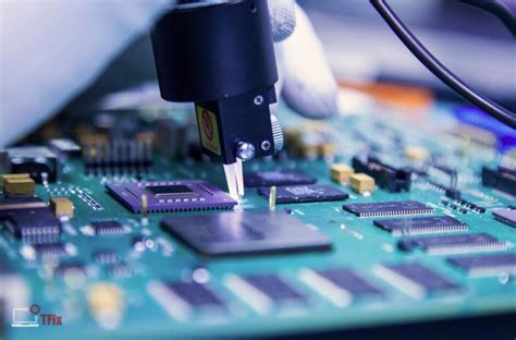
Visual Inspection: PCBs are visually inspected for defects such as scratches, dust particles, or incorrect component placement. Automated optical inspection (AOI) systems are commonly used for this purpose.
-
Electrical Testing: PCBs undergo electrical testing to verify the continuity and isolation of the copper traces. Flying probe testing and in-circuit testing (ICT) are commonly used methods.
-
Functional Testing: The assembled PCB is tested for its intended functionality to ensure that it meets the specified requirements.
-
Environmental Testing: PCBs may be subjected to environmental tests such as temperature cycling, humidity exposure, and vibration testing to assess their durability and reliability under different operating conditions.
-
X-ray Inspection: X-ray inspection is used to detect internal defects such as voids, cracks, or misaligned components in multi-layer PCBs.
| Test Method | Purpose |
|---|---|
| Visual Inspection | Detect surface defects and component placement issues |
| Electrical Testing | Verify continuity and isolation of copper traces |
| Functional Testing | Ensure PCB meets intended functionality requirements |
| Environmental Testing | Assess durability and reliability under various conditions |
| X-ray Inspection | Detect internal defects in multi-layer PCBs |

Standards and Certifications
To ensure consistency and reliability in PCB quality, various standards and certifications have been established:
IPC Standards
The Association Connecting Electronics Industries (IPC) is a global trade association that develops standards for the electronics industry. Some of the key IPC standards related to PCB quality include:
- IPC-A-600: Acceptability of Printed Boards
- IPC-6012: Qualification and Performance Specification for Rigid Printed Boards
- IPC-6013: Qualification and Performance Specification for Flexible Printed Boards
- IPC-A-610: Acceptability of Electronic Assemblies
These standards provide guidelines and acceptance criteria for various aspects of PCB fabrication and assembly.
UL Certification
Underwriters Laboratories (UL) is a global safety certification company that tests and certifies products, including PCBs, for safety and performance. UL offers several certifications relevant to PCBs, such as:
- UL 94: Standard for Safety of Flammability of Plastic Materials for Parts in Devices and Appliances
- UL 796: Standard for Safety of Printed-Wiring Boards
- UL 746E: Standard for Safety of Polymeric Materials – Industrial Laminates, Filament Wound Tubing, Vulcanized Fibre, and Materials Used in Printed-Wiring Boards
Obtaining UL certification demonstrates that the PCB meets the necessary safety and performance requirements.
ISO Certification
The International Organization for Standardization (ISO) develops and publishes international standards for various industries. ISO 9001 is a quality management system standard that applies to PCB manufacturers. It sets out the requirements for a quality management system that ensures consistent product quality and customer satisfaction.

Choosing a High-Quality PCB Manufacturer
Selecting a high-quality PCB manufacturer is crucial for ensuring the quality and reliability of your electronic products. Here are some key factors to consider when choosing a PCB manufacturer:
-
Experience and Expertise: Look for a manufacturer with a proven track record in producing high-quality PCBs for your specific industry or application.
-
Quality Management System: Ensure that the manufacturer has a robust quality management system in place, preferably certified to ISO 9001 standards.
-
Manufacturing Capabilities: Consider the manufacturer’s capabilities in terms of PCB complexity, layer count, material options, and surface finishes.
-
Testing and Inspection: Inquire about the manufacturer’s testing and inspection processes to ensure that they employ rigorous quality control measures.
-
Certifications and Compliance: Verify that the manufacturer holds the necessary certifications and complies with relevant industry standards, such as IPC and UL.
-
Customer Support: Evaluate the manufacturer’s responsiveness, communication, and technical support to ensure a smooth collaboration throughout the PCB development process.

FAQ
-
What is the difference between a single-sided and double-sided PCB?
A single-sided PCB has copper traces on only one side of the substrate, while a double-sided PCB has copper traces on both sides. Double-sided PCBs offer higher component density and more complex routing options. -
What is the purpose of a solder mask on a PCB?
The solder mask is a protective layer applied over the copper traces on a PCB. It serves to insulate the traces, prevent short circuits, and protect the PCB from environmental factors such as dust and moisture. -
What is the importance of impedance control in PCB design?
Impedance control is critical in high-speed PCB designs to ensure proper signal transmission and minimize signal distortion. By carefully controlling the impedance of the traces, designers can prevent signal reflections and maintain signal integrity. -
What are the common surface finishes used on PCBs?
Common surface finishes for PCBs include Hot Air Solder Leveling (HASL), Immersion Silver (IAg), Immersion Tin (ISn), and Electroless Nickel Immersion Gold (ENIG). Each surface finish has its own advantages in terms of cost, durability, and solderability. -
How can I ensure the quality of the PCBs I receive from a manufacturer?
To ensure the quality of PCBs, you can take the following steps: - Clearly communicate your requirements and specifications to the manufacturer.
- Request a detailed manufacturing and testing plan from the manufacturer.
- Specify the applicable industry standards and certifications for your PCBs.
- Conduct incoming quality control inspections upon receiving the PCBs.
- Establish a long-term partnership with a reputable PCB manufacturer.
Conclusion
PCB quality is a critical factor in the success of any electronic product. By understanding the various aspects of PCB quality, from design and material selection to manufacturing processes and quality control, you can ensure that your PCBs meet the highest standards of reliability and performance.
When selecting a PCB manufacturer, it is essential to consider their experience, capabilities, certifications, and commitment to quality. By partnering with a reputable manufacturer and following industry best practices, you can minimize the risk of PCB-related issues and ensure the long-term success of your electronic products.

Leave a Reply