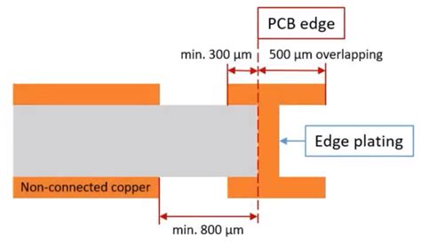
Why is PCB Edge Plating Used?
Protection Against Corrosion
One of the primary reasons for using PCB edge plating is to protect the exposed copper traces and layers from corrosion. When a PCB is manufactured, the edges of the board are often left exposed, leaving the copper vulnerable to oxidation and other environmental factors. By applying a layer of conductive metal, such as gold, silver, or tin, the edges are sealed and protected from corrosion.
Improved Electrical Conductivity
PCB edge plating also enhances the electrical conductivity of the circuit board. The plated metal layer creates a low-resistance path for electrical signals to travel along the edges of the board, ensuring optimal signal transmission and reducing the risk of signal loss or interference.
Enhanced Mechanical Strength
Edge plating can also improve the mechanical strength of a PCB. The additional metal layer helps to reinforce the edges of the board, making it more resistant to damage from handling, vibration, or impact. This is particularly important for PCBs used in high-stress environments, such as automotive or aerospace applications.
Improved Aesthetics
In addition to its functional benefits, PCB edge plating can also enhance the visual appearance of the circuit board. A shiny, metallic edge can give the PCB a more polished and professional look, which may be desirable for certain applications or products.
PCB Edge Plating Processes
There are several methods for applying edge plating to a PCB, each with its own advantages and limitations. The choice of process depends on factors such as the desired thickness of the plating, the type of metal being used, and the specific requirements of the application.
Electroless Plating
Electroless plating is a chemical process that deposits a thin layer of metal onto the edges of the PCB without the use of an electric current. This method typically involves immersing the board in a series of chemical baths that contain the plating solution and activators. The most common metals used in electroless plating are nickel and gold.
Advantages of electroless plating include:
– Uniform coverage, even on complex or irregular shapes
– No electrical connection required
– Suitable for non-conductive substrates
Limitations of electroless plating include:
– Relatively thin plating layers (typically 1-5 microns)
– Slower deposition rates compared to electrolytic plating
– Higher material costs
Electrolytic Plating
Electrolytic plating, also known as electroplating, uses an electric current to deposit a layer of metal onto the edges of the PCB. The board is placed in an electrolytic bath containing the plating solution, and an electrical current is applied, causing the metal ions to bond to the exposed copper on the board edges.
Advantages of electrolytic plating include:
– Thicker plating layers (up to 100 microns or more)
– Faster deposition rates compared to electroless plating
– Lower material costs
Limitations of electrolytic plating include:
– Requires an electrical connection to the board
– May not provide uniform coverage on complex or irregular shapes
– Limited to conductive substrates
Comparison of Plating Processes
| Process | Thickness | Coverage | Speed | Cost |
|---|---|---|---|---|
| Electroless | Thin (1-5 µm) | Uniform | Slow | High |
| Electrolytic | Thick (up to 100 µm) | May be uneven | Fast | Low |
Selecting the Right PCB Edge Plating
When choosing a PCB edge plating method and material, several factors must be considered to ensure the best performance and durability for the specific application.
Plating Material
The choice of plating material depends on the desired properties and the operating environment of the PCB. Common materials include:
- Gold: Offers excellent corrosion resistance and electrical conductivity, but is expensive.
- Silver: Provides good conductivity and is less expensive than gold, but has lower corrosion resistance.
- Tin: Offers good solderability and is less expensive than gold or silver, but has lower conductivity and corrosion resistance.
- Nickel: Provides good mechanical strength and is often used as an underlayer for other plating materials.
Plating Thickness
The thickness of the edge plating layer affects the mechanical strength, electrical conductivity, and cost of the PCB. Thicker layers offer better protection and conductivity but also increase the overall cost and may require additional processing steps.
Typical plating thicknesses range from 1 to 100 microns, depending on the application and the plating process used.
Environmental Factors
The operating environment of the PCB should also be considered when selecting the edge plating material and process. Factors such as temperature, humidity, and exposure to corrosive substances can affect the performance and durability of the plating.
For example, PCBs used in outdoor or marine environments may require more robust corrosion protection, such as thicker gold plating, while those used in controlled indoor environments may be able to use less expensive materials like tin.

PCB Edge Plating Standards and Specifications
Several industry standards and specifications provide guidelines for PCB edge plating to ensure consistent quality and performance.
IPC Standards
The IPC (Association Connecting Electronics Industries) publishes several standards related to PCB edge plating, including:
- IPC-4552: Specification for Electroless Nickel/Immersion Gold (ENIG) Plating for Printed Circuit Boards
- IPC-4553: Specification for Immersion Silver Plating for Printed Circuit Boards
- IPC-4554: Specification for Immersion Tin Plating for Printed Circuit Boards
These standards define requirements for plating thickness, coverage, adhesion, and other quality characteristics.
Military and Aerospace Specifications
PCBs used in military and aerospace applications often have more stringent requirements for edge plating due to the harsh operating environments and high reliability demands. Relevant specifications include:
- MIL-PRF-31032: Performance Specification for Printed Circuit Board/Printed Wiring Board, General Specification for
- MIL-PRF-55110: Performance Specification for Printed Wiring Board, Rigid, General Specification for
These specifications may require thicker plating layers, specific materials, or additional testing and inspection procedures.
Frequently Asked Questions (FAQ)
-
What is the purpose of PCB edge plating?
PCB edge plating serves several purposes, including protection against corrosion, improved electrical conductivity, enhanced mechanical strength, and improved aesthetics. -
What materials are commonly used for PCB edge plating?
Common materials for PCB edge plating include gold, silver, tin, and nickel. The choice of material depends on the desired properties and the operating environment of the PCB. -
What are the differences between electroless and electrolytic plating?
Electroless plating is a chemical process that deposits a thin layer of metal without the use of an electric current, while electrolytic plating uses an electric current to deposit a thicker layer of metal. Electroless plating provides more uniform coverage but is slower and more expensive, while electrolytic plating is faster and less expensive but may not provide uniform coverage on complex shapes. -
How thick should the PCB edge plating be?
The thickness of the PCB edge plating depends on the application and the desired properties. Typical thicknesses range from 1 to 100 microns, with thicker layers offering better protection and conductivity but also increasing cost. -
Are there any industry standards for PCB edge plating?
Yes, several industry standards provide guidelines for PCB edge plating, including IPC standards (IPC-4552, IPC-4553, IPC-4554) and military/aerospace specifications (MIL-PRF-31032, MIL-PRF-55110). These standards define requirements for plating thickness, coverage, adhesion, and other quality characteristics.
Conclusion
PCB edge plating is a crucial process in the manufacturing of printed circuit boards, offering protection against corrosion, improved electrical conductivity, enhanced mechanical strength, and improved aesthetics. The choice of plating material, thickness, and process depends on the specific application and operating environment of the PCB.
By understanding the various plating methods, materials, and industry standards, designers and manufacturers can select the most appropriate edge plating solution for their PCBs, ensuring optimal performance, reliability, and durability.
Leave a Reply