The Purpose of General Purpose PCBs
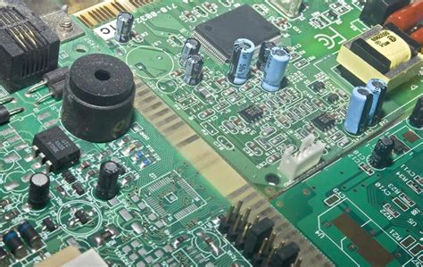
The primary purpose of a general purpose PCB is to provide a platform for mounting and interconnecting electronic components in a manner that enables the desired functionality of an electronic device. These PCBs serve as the foundation for creating electronic circuits and systems across various industries and applications.
Versatility and Adaptability
One of the key purposes of general purpose PCBs is their versatility and adaptability. These PCBs are designed to accommodate a wide range of electronic components, including:
- Resistors
- Capacitors
- Inductors
- Diodes
- Transistors
- Integrated circuits (ICs)
By providing a platform that can support diverse components, general purpose PCBs enable engineers and designers to create custom electronic circuits tailored to their specific requirements.
Cost-effectiveness
Another essential purpose of general purpose PCBs is their cost-effectiveness. Since these PCBs are not designed for a specific application, they can be mass-produced, resulting in lower manufacturing costs compared to custom-designed PCBs. This cost-effectiveness makes general purpose PCBs an attractive choice for projects with budget constraints or for prototyping purposes.
Characteristics of General Purpose PCBs
General purpose PCBs possess several key characteristics that distinguish them from other types of PCBs. These characteristics contribute to their versatility and wide-ranging applications.
Layered Structure
General purpose PCBs typically consist of multiple layers of conductive and insulating materials. The most common layer configurations are:
| Layers | Description |
|---|---|
| Single-layer | One conductive layer, typically used for simple circuits |
| Double-layer | Two conductive layers, allowing for more complex circuits and better signal integrity |
| Multi-layer | Three or more conductive layers, enabling even more complex designs and improved performance |
The number of layers in a general purpose PCB depends on the complexity of the electronic circuit and the desired functionality.
Copper Traces and Pads
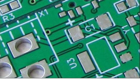
The conductive layers of a general purpose PCB are made of copper, which is an excellent conductor of electricity. The copper is etched into traces and pads that form the electrical connections between components. The width and thickness of these traces and pads are designed to accommodate the current and power requirements of the electronic components.
Solder Mask and Silkscreen
To protect the copper traces and pads from oxidation and short-circuits, a solder mask layer is applied to the PCB. This layer is typically green in color but can also be found in other colors such as red, blue, or black. Additionally, a silkscreen layer is added to the PCB to provide text and symbols that aid in the assembly and identification of components.

Manufacturing Process of General Purpose PCBs
The manufacturing process of general purpose PCBs involves several steps that ensure the quality and reliability of the final product.
Design and Fabrication
-
PCB Design: The first step in the manufacturing process is the design of the PCB. Engineers use specialized software to create a schematic diagram and a PCB layout that defines the placement of components and the routing of copper traces.
-
Fabrication: Once the design is finalized, the fabrication process begins. This involves the following sub-steps:
- Substrate preparation: A substrate material, typically FR-4 (a glass-reinforced epoxy laminate), is cut to the desired size and shape.
- Copper lamination: Copper foil is laminated onto the substrate using heat and pressure.
- Drilling: Holes are drilled into the PCB for through-hole components and vias.
- Plating: The drilled holes are plated with copper to create electrical connections between layers.
- Etching: The unwanted copper is removed using a chemical etching process, leaving behind the desired traces and pads.
- Solder mask application: A solder mask layer is applied to protect the copper traces and pads.
- Silkscreen printing: The silkscreen layer is printed onto the PCB for component identification and assembly guidance.
Assembly and Testing
After the fabrication process, the general purpose PCB is ready for assembly and testing.
-
Component Placement: The electronic components are placed onto the PCB either manually or using automated pick-and-place machines. The components are positioned according to the PCB layout and soldered onto the pads.
-
Soldering: The PCB is then sent through a reflow oven or wave soldering machine to permanently attach the components to the board. The solder melts and forms a strong electrical and mechanical bond between the components and the PCB.
-
Inspection and Testing: After the soldering process, the assembled PCB undergoes visual inspection and automated optical inspection (AOI) to identify any manufacturing defects or component placement issues. Electrical testing is also performed to ensure that the PCB Functions as intended.
-
Finishing: Finally, any required surface finishes, such as conformal coating or potting, are applied to the PCB to provide additional protection against environmental factors.

Applications of General Purpose PCBs
General purpose PCBs find applications in a wide range of industries and electronic devices. Some common applications include:
-
Consumer Electronics: General purpose PCBs are used in various consumer electronic devices, such as smartphones, tablets, laptops, televisions, and home appliances. These PCBs provide the necessary interconnections and support for the electronic components within these devices.
-
Industrial Electronics: In industrial settings, general purpose PCBs are employed in control systems, automation equipment, sensors, and data acquisition devices. These PCBs are designed to withstand harsh environments and provide reliable performance.
-
Medical Devices: General purpose PCBs are used in medical electronic devices, such as patient monitors, imaging equipment, and diagnostic tools. These PCBs must meet strict quality and reliability standards to ensure patient safety and accurate medical readings.
-
Automotive Electronics: In the automotive industry, general purpose PCBs are used in various electronic systems, including engine control units (ECUs), infotainment systems, and advanced driver assistance systems (ADAS). These PCBs are designed to withstand the vibrations, temperature fluctuations, and electromagnetic interference present in automotive environments.
-
Aerospace and Defense: General purpose PCBs are employed in aerospace and defense applications, such as avionics systems, communication equipment, and surveillance devices. These PCBs are subject to rigorous testing and certification to ensure reliable operation in extreme conditions.
-
IoT and Wearables: With the growth of the Internet of Things (IoT) and wearable technology, general purpose PCBs have found new applications in connected devices, sensors, and smart wearables. These PCBs are designed to be compact, low-power, and capable of wireless communication.

FAQ
-
Q: Can general purpose PCBs be customized for specific applications?
A: Yes, general purpose PCBs can be customized to some extent by selecting the appropriate layer configuration, copper thickness, and surface finish to meet the specific requirements of an application. However, for highly specialized applications, custom-designed PCBs may be more suitable. -
Q: What is the typical turnaround time for manufacturing general purpose PCBs?
A: The turnaround time for manufacturing general purpose PCBs depends on various factors, such as the complexity of the design, the number of layers, and the quantity ordered. Typically, small-volume orders can be manufactured within 1-2 weeks, while larger orders may take several weeks. -
Q: Are general purpose PCBs suitable for high-frequency applications?
A: General purpose PCBs can be used for high-frequency applications, but they may require specific design considerations, such as controlled impedance, minimized crosstalk, and proper grounding techniques. In some cases, specialized high-frequency PCB materials, such as Rogers or Teflon, may be necessary to achieve the desired performance. -
Q: How do I select the appropriate general purpose PCB for my project?
A: When selecting a general purpose PCB for your project, consider factors such as the number of layers required, the size and complexity of the electronic circuit, the power and current requirements, and the operating environment. Consult with a PCB manufacturer or an experienced electronics engineer to determine the most suitable PCB specifications for your application. -
Q: Can general purpose PCBs be used for prototyping?
A: Yes, general purpose PCBs are commonly used for prototyping purposes. They provide a cost-effective and efficient way to test and validate electronic designs before proceeding with large-scale production. Prototyping with general purpose PCBs allows for iterative design improvements and helps identify any potential issues early in the development process.
Conclusion
General purpose PCBs are an essential component in the world of electronics, serving as the foundation for a wide range of electronic devices and systems. Their versatility, cost-effectiveness, and reliability make them a popular choice for engineers and designers across various industries. By understanding the purpose, characteristics, manufacturing process, and applications of general purpose PCBs, one can appreciate their significance in enabling the functionality and performance of modern electronic devices. As technology continues to evolve, general purpose PCBs will undoubtedly play a crucial role in shaping the future of electronics.

Leave a Reply