Introduction to AOI in PCB Manufacturing
Automated Optical Inspection (AOI) is a crucial technology used in the manufacturing of Printed Circuit Boards (PCBs) to ensure quality control and detect defects. In the highly competitive and quality-driven electronics industry, AOI has become an indispensable tool for manufacturers to maintain high standards and reduce costs associated with defective products.
What is a PCB?
A Printed Circuit Board (PCB) is a fundamental component in modern electronics. It is a flat board made of insulating materials, such as fiberglass or composite epoxy, with conductive pathways etched or printed onto its surface. These pathways, known as traces, connect various electronic components, such as resistors, capacitors, and integrated circuits, to create a functional electronic device.
PCBs play a vital role in the electronics industry, as they are used in a wide range of applications, from consumer electronics and automotive systems to aerospace and medical devices. The complexity and density of PCBs have increased significantly over the years, making it more challenging to ensure their quality and reliability.
The Need for Automated Optical Inspection
As PCBs become more complex and miniaturized, the likelihood of defects occurring during the manufacturing process increases. These defects can range from minor issues, such as solder bridging or component misalignment, to more severe problems, like open circuits or short circuits. Even a single defect can render the entire PCB useless, leading to costly rework or scrap.
Traditionally, PCB inspection was performed manually by trained operators using microscopes or magnifying glasses. However, this method is time-consuming, labor-intensive, and prone to human error. As the demand for high-quality PCBs grew, manufacturers sought ways to automate the inspection process, leading to the development of AOI systems.
How AOI Works in PCB Inspection
The Basics of AOI Technology
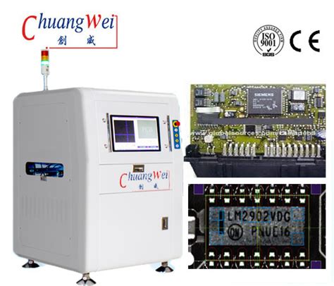
Automated Optical Inspection systems use advanced imaging technology, such as high-resolution cameras and image processing algorithms, to capture and analyze images of PCBs at various stages of the manufacturing process. These systems compare the captured images to a pre-defined set of design data, known as the golden sample or reference image, to identify any discrepancies or defects.
AOI systems typically consist of the following components:
- Illumination system: Provides consistent and uniform lighting conditions to ensure accurate image capture.
- Imaging system: High-resolution cameras capture images of the PCB from various angles and magnifications.
- Image processing software: Analyzes the captured images using algorithms to detect defects and compare them to the reference data.
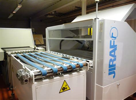
- Conveyor system: Transports the PCBs through the AOI machine for inspection.
- User interface: Allows operators to monitor the inspection process, review defects, and generate reports.
Types of AOI Systems
There are two main types of AOI systems used in PCB manufacturing:
-
2D AOI: These systems use two-dimensional imaging to inspect the PCB from a top-down view. They are effective in detecting surface-level defects, such as component placement, solder joint quality, and trace integrity. However, they may have limitations in detecting defects in tall components or hidden areas.
-
3D AOI: These systems use three-dimensional imaging techniques, such as laser triangulation or structured light, to create a 3D model of the PCB. This allows for the inspection of defects that may be hidden from a 2D perspective, such as lifted leads or component height variations. 3D AOI systems provide more comprehensive inspection capabilities but are generally more expensive than 2D systems.
Advantages of AOI in PCB Manufacturing
Implementing AOI in PCB manufacturing offers several benefits, including:
-
Increased efficiency: AOI systems can inspect PCBs much faster than manual inspection, allowing for higher throughput and reduced production time.
-
Improved accuracy: AOI systems are not subject to human fatigue or subjectivity, resulting in more consistent and reliable defect detection.
-
Early defect detection: By inspecting PCBs at various stages of the manufacturing process, AOI can identify defects early on, reducing the risk of defective products reaching later stages or the end customer.
-
Cost reduction: Early defect detection and improved accuracy help reduce the costs associated with rework, scrap, and warranty claims.
-
Traceable quality data: AOI systems generate detailed inspection reports and data, which can be used for quality analysis, process improvement, and traceability purposes.

Common PCB Defects Detected by AOI
AOI systems are designed to detect a wide range of defects that can occur during PCB manufacturing. Some of the most common defects include:
Solder Defects
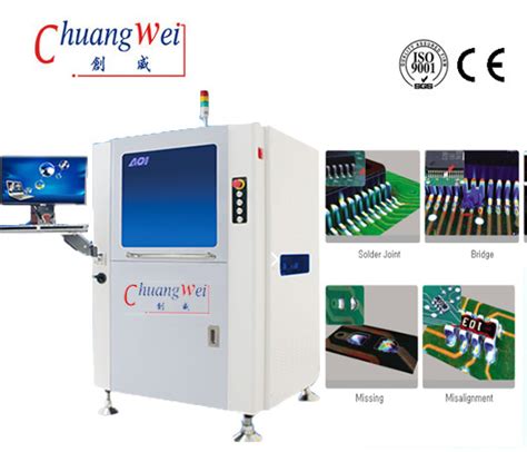
- Solder bridges: Unintended connections between two or more solder joints, causing short circuits.
- Solder voids: Gaps or holes within the solder joint, weakening the connection and potentially leading to failure.
- Insufficient or excess solder: Too little or too much solder on a joint, affecting its mechanical and electrical properties.
Component Defects
- Missing components: Components that are not placed on the PCB as per the design.
- Misaligned components: Components that are not properly aligned with their designated pads or footprints.
- Incorrect component polarity or orientation: Components that are placed with the wrong polarity or orientation, potentially causing functional issues.
Trace and Pad Defects
- Open circuits: Broken or disconnected traces, preventing electrical continuity.
- Short circuits: Unintended connections between traces or pads, causing electrical shorts.
- Trace width or spacing violations: Traces that are too narrow or too close to each other, not meeting the design specifications.
Other Defects
- Foreign material: Debris or contaminants on the PCB surface that can cause short circuits or affect component placement.
- Markings and labeling: Incorrect or missing markings, such as part numbers or polarity indicators.
- Dimensional defects: PCB features that do not meet the specified dimensions, such as hole size or edge clearance.
By detecting these defects early in the manufacturing process, AOI helps ensure that only high-quality PCBs proceed to the next stages of assembly or shipment.

Implementing AOI in PCB Manufacturing
Selecting the Right AOI System
When considering implementing AOI in a PCB manufacturing facility, it is essential to select the right system based on the specific needs and requirements of the production process. Factors to consider include:
-
PCB complexity: The complexity of the PCBs being manufactured will determine the type of AOI system required, such as 2D or 3D, and the level of resolution and accuracy needed.
-
Production volume: The throughput requirements and production volume will influence the speed and capacity of the AOI system needed.
-
Defect types: The most common or critical defect types encountered in the manufacturing process should be considered when selecting an AOI system to ensure it can effectively detect and classify those defects.
-
Integration with existing processes: The AOI system should be compatible with existing manufacturing equipment and software systems to ensure seamless integration and data exchange.
-
Budget and ROI: The cost of the AOI system and its expected return on investment (ROI) should be evaluated to justify the implementation and ensure long-term benefits.
Best Practices for AOI Implementation
To maximize the benefits of AOI in PCB manufacturing, consider the following best practices:
-
Establish clear inspection criteria: Define the defect types, thresholds, and acceptance criteria for the AOI system based on industry standards, customer requirements, and internal quality goals.
-
Develop a comprehensive library: Create and maintain a library of component models, footprints, and reference images to ensure accurate defect detection and classification.
-
Regular calibration and maintenance: Implement a regular calibration and maintenance schedule for the AOI system to ensure consistent performance and minimize downtime.
-
Operator training: Provide adequate training to operators on the proper use, maintenance, and troubleshooting of the AOI system.
-
Continuous improvement: Regularly analyze AOI data and use it to identify areas for process improvement, such as optimizing solder paste application or component placement parameters.
Integrating AOI with Other Quality Control Methods
While AOI is a powerful tool for PCB inspection, it should not be relied upon as the sole quality control method. Integrating AOI with other inspection techniques can provide a more comprehensive approach to ensuring PCB quality. Some complementary methods include:
-
In-Circuit Testing (ICT): Electrical testing of the PCB to verify the functionality and connectivity of components.
-
Functional Testing: Testing the PCB under real-world operating conditions to ensure it meets the desired performance specifications.
-
X-ray Inspection: Non-destructive testing method that can reveal defects hidden from view, such as voids in ball grid array (BGA) solder joints.
-
Visual Inspection: Manual inspection of PCBs by trained operators to identify defects that may not be detectable by AOI, such as subtle cosmetic issues.
By combining AOI with these other quality control methods, manufacturers can achieve a higher level of confidence in the quality and reliability of their PCBs.

Frequently Asked Questions (FAQ)
- What is the difference between 2D and 3D AOI systems?
-
2D AOI systems use two-dimensional imaging to inspect PCBs from a top-down view, while 3D AOI systems use three-dimensional imaging techniques to create a 3D model of the PCB, allowing for the detection of defects hidden from a 2D perspective.
-
Can AOI replace manual visual inspection entirely?
-
While AOI can significantly reduce the need for manual visual inspection, it should not be relied upon as the sole quality control method. Integration with other inspection techniques, including manual visual inspection, can provide a more comprehensive approach to ensuring PCB quality.
-
How does AOI handle the inspection of different component types and sizes?
-
AOI systems use a library of component models and footprints to accurately detect and classify defects. This library must be regularly updated to include new component types and sizes as they are introduced into the manufacturing process.
-
What are the main benefits of implementing AOI in PCB manufacturing?
-
The main benefits of AOI include increased inspection efficiency, improved defect detection accuracy, early identification of defects, reduced costs associated with rework and scrap, and the generation of traceable quality data for process improvement.
-
How often should an AOI system be calibrated and maintained?
- The frequency of calibration and maintenance for an AOI system depends on factors such as the system type, usage, and manufacturer recommendations. Generally, regular calibration and maintenance should be performed to ensure consistent performance and minimize downtime. It is essential to follow the manufacturer’s guidelines and establish a schedule that meets the specific needs of the production environment.
Conclusion
Automated Optical Inspection (AOI) has become an essential technology in PCB manufacturing, enabling manufacturers to ensure the quality and reliability of their products while reducing costs and improving efficiency. By detecting a wide range of defects early in the production process, AOI helps prevent defective PCBs from reaching later stages of assembly or the end customer.
When implementing AOI, it is crucial to select the right system based on specific manufacturing needs, establish clear inspection criteria, and integrate AOI with other quality control methods for a comprehensive approach to PCB quality assurance. Regular maintenance, operator training, and continuous process improvement are also key factors in maximizing the benefits of AOI.
As PCB complexity continues to increase and the demand for high-quality electronics grows, the role of AOI in PCB manufacturing will become even more critical. By embracing this technology and following best practices, manufacturers can position themselves to meet the evolving needs of the industry and deliver products that meet the highest standards of quality and reliability.

Leave a Reply