Introduction to Circuit Boards
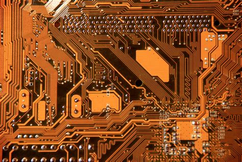
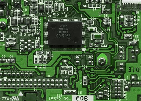
A circuit board, also known as a printed circuit board (PCB), is the backbone of most electronic devices. It is a flat board made of insulating material, such as fiberglass or plastic, with conductive pathways etched or printed onto its surface. These pathways, called traces, connect various electronic components, such as resistors, capacitors, and integrated circuits (ICs), to create a functional electronic circuit.
What are the Basic Components of a Circuit Board?
| Component | Function |
|---|---|
| Substrate | The insulating base material, usually made of fiberglass or plastic |
| Copper Traces | Conductive pathways that connect components |
| Solder Mask | A protective layer that covers the copper traces, leaving only the connection points exposed |
| Silkscreen | A printed layer that adds labels, logos, and component outlines for easier assembly and debugging |
| Vias | Conductive holes that allow traces to connect between layers of a multi-layer PCB |
| Pads | Exposed areas of copper where components are soldered |
Types of Circuit Boards
There are several types of circuit boards, each with its own unique characteristics and applications.
Single-Layer PCBs
Single-layer PCBs, also known as single-sided PCBs, have conductive traces on only one side of the substrate. These boards are the simplest and most affordable to manufacture, making them ideal for low-complexity projects and prototypes. However, their limited routing options and lower component density make them less suitable for more advanced applications.
Double-Layer PCBs
Double-layer PCBs, or double-sided PCBs, have conductive traces on both sides of the substrate. This allows for more complex routing and higher component density compared to single-layer boards. The two layers are connected using vias, which are conductive holes drilled through the board. Double-layer PCBs are commonly used in a wide range of electronic devices, from consumer electronics to industrial control systems.
Multi-Layer PCBs
Multi-layer PCBs have three or more conductive layers, with insulating layers separating them. These boards offer the highest level of complexity and component density, making them suitable for advanced applications such as high-speed digital circuits, RF devices, and aerospace systems. The multiple layers allow for intricate routing, better signal integrity, and improved electromagnetic compatibility (EMC).
Flexible PCBs
Flexible PCBs, or flex circuits, are made using a flexible substrate material, such as polyimide or polyester. These boards can bend and twist without damaging the conductive traces, making them ideal for applications that require flexibility or need to fit into tight spaces. Flex circuits are commonly found in wearable devices, medical equipment, and automotive electronics.
Rigid-Flex PCBs
Rigid-flex PCBs combine the benefits of both rigid and flexible PCBs. They consist of rigid PCB sections connected by flexible PCB sections, allowing for three-dimensional packaging and improved reliability in applications that require both stability and flexibility. Rigid-flex PCBs are often used in aerospace, military, and medical devices.
PCB Manufacturing Process
The PCB manufacturing process involves several steps, each crucial to ensuring the quality and functionality of the final product.
Design and Layout
The first step in PCB manufacturing is designing the circuit schematic and creating the PCB layout using specialized software. The layout determines the placement of components and the routing of conductive traces, taking into account factors such as signal integrity, power distribution, and manufacturability.
PCB Fabrication
Once the design is finalized, the PCB fabrication process begins. This involves the following steps:
- Substrate preparation: The base material is cut to size and cleaned.
- Copper cladding: A thin layer of copper is laminated onto the substrate.
- Photoresist application: A light-sensitive film is applied to the copper layer.
- Exposure and development: The photoresist is exposed to UV light through a photomask, which hardens the exposed areas. The unexposed areas are then removed using a developer solution.
- Etching: The exposed copper is removed using an etchant solution, leaving only the desired conductive traces.
- Solder mask application: A protective layer is applied to the board, covering the traces but leaving the pads exposed.
- Silkscreen printing: Labels, logos, and component outlines are printed onto the solder mask.
- Surface finish: A protective coating, such as HASL (Hot Air Solder Leveling) or ENIG (Electroless Nickel Immersion Gold), is applied to the exposed pads to prevent oxidation and improve solderability.
PCB Assembly
After the PCB fabrication is complete, the electronic components are assembled onto the board. This can be done manually for low-volume production or prototyping, but high-volume manufacturing typically uses automated assembly processes, such as surface mount technology (SMT) or through-hole technology (THT).
- Solder paste application: For SMT assembly, a thin layer of solder paste is applied to the pads using a stencil.
- Component placement: Components are placed onto the board, either manually or using a pick-and-place machine.
- Reflow soldering: The board is heated in a reflow oven, melting the solder paste and creating a permanent connection between the components and the pads.
- Through-hole component insertion: For THT assembly, through-hole components are inserted into the board manually or using automated insertion machines.
- Wave soldering: The board is passed over a wave of molten solder, which fills the through-holes and creates a connection between the components and the pads.
Testing and Inspection
After assembly, the PCBs undergo various testing and inspection processes to ensure their quality and functionality. These may include:
- Visual inspection: Checking for proper component placement, solder joint quality, and any visible defects.
- Automated optical inspection (AOI): Using machine vision to detect assembly defects.
- X-ray inspection: Examining solder joints and internal structures for hidden defects.
- In-circuit testing (ICT): Verifying the presence and functionality of individual components.
- Functional testing: Checking the overall performance of the assembled PCB against its specifications.

Applications of Circuit Boards
Circuit boards are used in virtually every electronic device, from simple consumer gadgets to complex industrial and aerospace systems. Some common applications include:
- Consumer electronics: Smartphones, tablets, laptops, televisions, and home appliances.
- Automotive electronics: Engine control units, infotainment systems, and advanced driver assistance systems (ADAS).
- Medical devices: Diagnostic equipment, patient monitoring systems, and implantable devices.
- Industrial control systems: Programmable logic controllers (PLCs), sensors, and automation equipment.
- Aerospace and defense: Avionics, communication systems, and weapons control systems.
- IoT devices: Smart home devices, wearables, and remote monitoring systems.
Future Trends in Circuit Board Technology
As electronic devices continue to advance, circuit board technology must evolve to keep pace with the growing demands for performance, miniaturization, and sustainability.
Advanced Materials
Researchers are exploring new substrate materials, such as ceramic, metal-core, and carbon-based composites, to improve thermal management, signal integrity, and mechanical stability. These materials could enable the development of high-performance PCBs for demanding applications, such as 5G communication, power electronics, and aerospace systems.
Embedded Components
Embedded component technology involves integrating passive components, such as resistors and capacitors, directly into the PCB substrate. This approach reduces the board size, improves signal integrity, and simplifies the assembly process. As the demand for miniaturization and high-density packaging grows, embedded component technology is expected to become more prevalent in PCB design and manufacturing.
3D Printing
Additive manufacturing, or 3D printing, is emerging as a potential game-changer in PCB fabrication. This technology allows for the creation of complex, three-dimensional PCB structures with embedded components and unique geometries. 3D-printed PCBs could enable rapid prototyping, customization, and the development of novel electronic devices with improved performance and functionality.
Sustainable Manufacturing
As environmental concerns gain prominence, the electronics industry is focusing on developing sustainable PCB manufacturing practices. This includes the use of eco-friendly materials, such as halogen-free substrates and lead-free solders, as well as the adoption of green manufacturing processes that minimize waste and energy consumption. Recycling and proper disposal of end-of-life PCBs are also crucial for reducing the environmental impact of electronic waste.
Frequently Asked Questions (FAQ)
-
What is the difference between a PCB and a circuit board?
A PCB (printed circuit board) is a specific type of circuit board that has conductive traces printed or etched onto its surface. The term “circuit board” is a more general term that encompasses various types of boards, including PCBs, breadboards, and stripboards. In common usage, however, the terms PCB and circuit board are often used interchangeably. -
Can I design and manufacture my own PCBs at home?
Yes, it is possible to design and manufacture simple PCBs at home using readily available tools and materials. For design, you can use free PCB design software, such as KiCad or Eagle. For manufacturing, you can use a toner transfer method or a chemical etching process to create the conductive traces on a copper-clad board. However, for more complex or high-quality PCBs, it is recommended to use professional PCB fabrication services. -
How do I choose the right type of PCB for my project?
The choice of PCB type depends on several factors, such as the complexity of the circuit, the required component density, the operating environment, and the budget. Single-layer PCBs are suitable for simple, low-cost projects, while double-layer and multi-layer PCBs are better for more complex circuits with higher component counts. Flexible and rigid-flex PCBs are ideal for applications that require flexibility or unique form factors. -
What is the typical turnaround time for PCB manufacturing?
The turnaround time for PCB manufacturing varies depending on the complexity of the design, the chosen fabrication service, and the manufacturing options selected (e.g., PCB material, surface finish, and testing requirements). For simple PCBs, the turnaround time can be as short as 24 hours for expedited services, while more complex boards may take several weeks. On average, most PCB fabrication services offer a turnaround time of 1-2 weeks for standard orders. -
How can I ensure the quality and reliability of my PCBs?
To ensure the quality and reliability of your PCBs, consider the following best practices: - Follow good PCB design guidelines, such as proper component placement, trace routing, and power distribution.
- Choose reputable PCB fabrication and assembly services with proven quality control processes.
- Specify appropriate manufacturing options, such as PCB material, surface finish, and testing requirements, based on your application’s needs.
- Conduct thorough testing and inspection of the assembled PCBs, including visual inspection, automated optical inspection (AOI), and functional testing.
- Implement proper handling, storage, and packaging procedures to prevent damage during transportation and use.
Conclusion
Circuit boards are the foundation of modern electronic devices, enabling the interconnection and functionality of various components. Understanding the types, manufacturing processes, and applications of circuit boards is crucial for anyone involved in electronics design, manufacturing, or troubleshooting.
As technology advances, circuit board design and manufacturing must adapt to meet the growing demands for performance, miniaturization, and sustainability. By staying informed about the latest trends and best practices in PCB technology, engineers and enthusiasts can create innovative electronic solutions that shape the future of our increasingly connected world.
Leave a Reply