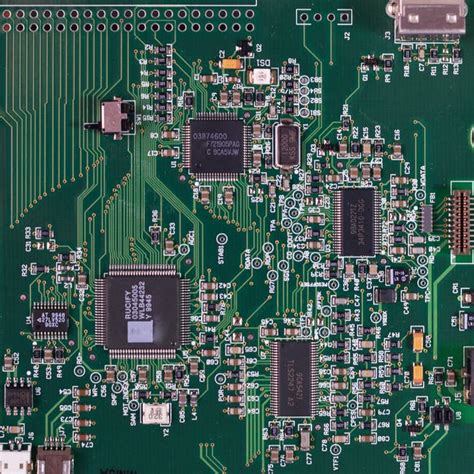
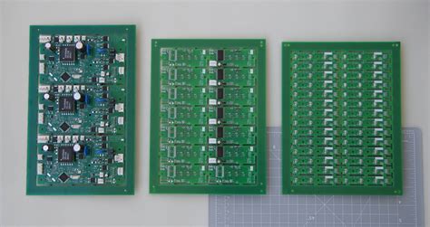
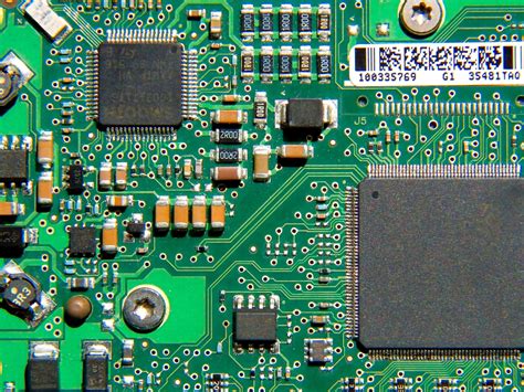
What is a circuit board?
A circuit board is a flat insulating board that holds and connects electronic components using conductive pathways, tracks, or signal traces etched from copper sheets laminated onto a non-conductive substrate. The primary purpose of a PCB is to mechanically support and electrically connect electronic components using conductive paths, tracks, or signal traces.
Key functions of a circuit board
1. Mechanical support
One of the primary functions of a circuit board is to provide mechanical support for electronic components. The PCB acts as a stable platform on which components can be securely mounted, ensuring they remain in place despite any vibrations or shocks the device may experience. This is particularly important for devices that are subject to frequent movement or harsh environments.
2. Electrical connectivity
The conductive pathways etched onto the PCB allow for the transmission of electrical signals and power between components. These pathways, known as traces, are designed to minimize interference and ensure optimal signal integrity. The layout of these traces is crucial to the proper functioning of the device, as it determines the flow of electricity and the interaction between components.
3. Heat dissipation
As electronic components operate, they generate heat. If this heat is not properly dissipated, it can lead to component failure and device malfunction. PCBs play a vital role in heat dissipation by providing a means for heat to be transferred away from sensitive components. This is often achieved through the use of heat sinks, which are mounted directly onto the PCB and help to distribute heat evenly across the board.
4. Electromagnetic interference (EMI) reduction
Electromagnetic interference (EMI) can cause significant problems in electronic devices, leading to signal degradation and potential malfunctions. PCBs help to reduce EMI by incorporating shielding techniques and proper trace layout. By minimizing the loop area of current paths and using ground planes, PCBs can effectively reduce the amount of EMI emitted by the device.
5. Size reduction and optimization
PCBs allow for the miniaturization of electronic devices by providing a compact and efficient means of connecting components. By using multi-layer boards and high-density layouts, designers can create devices that are smaller, lighter, and more portable than ever before. This is particularly important in industries such as consumer electronics, where device size and weight are critical factors in market success.

Types of circuit boards
There are several types of circuit boards, each with its own unique characteristics and applications. The most common types include:
| Type | Layers | Application |
|---|---|---|
| Single-layer | 1 | Simple, low-cost devices |
| Double-layer | 2 | Most common, used in a wide range of devices |
| Multi-layer | 3+ | Complex devices requiring high component density |
| Flexible | Varies | Devices requiring flexibility or unconventional shapes |
| Rigid-flex | Varies | Devices requiring both rigid and flexible sections |
Single-layer PCBs
Single-layer PCBs consist of a single copper layer on one side of the substrate. They are the simplest and most cost-effective type of PCB, making them ideal for low-complexity devices or prototyping purposes. However, their limited connectivity and lack of EMI shielding make them unsuitable for more advanced applications.
Double-layer PCBs
Double-layer PCBs have copper layers on both sides of the substrate, allowing for greater connectivity and component density compared to single-layer boards. They are the most commonly used type of PCB, found in a wide range of electronic devices. The two layers are connected using through-hole technology or vias.
Multi-layer PCBs
Multi-layer PCBs consist of three or more conductive layers separated by insulating layers. These boards offer the highest level of connectivity and component density, making them ideal for complex devices such as smartphones, computers, and medical equipment. The increased number of layers also provides better EMI shielding and improved signal integrity.
Flexible PCBs
Flexible PCBs, as the name suggests, are designed to be flexible and can be bent or folded to fit into unconventional spaces. They are made using a flexible substrate material, such as polyimide, and are often used in devices that require flexibility or must conform to unique shapes. Examples include wearable electronics, medical implants, and aerospace applications.
Rigid-flex PCBs
Rigid-flex PCBs combine the benefits of both rigid and flexible PCBs. They consist of rigid sections connected by flexible sections, allowing for three-dimensional shaping and improved reliability in devices that require both stability and flexibility. Rigid-flex PCBs are commonly used in aerospace, military, and high-end consumer electronics applications.

The PCB manufacturing process
The manufacturing process for PCBs involves several steps, each of which is critical to ensuring the quality and reliability of the final product. The main steps include:
- Design and layout
- Substrate preparation
- Copper foil lamination
- Photoresist application
- Exposure and development
- Etching
- Drilling
- Plating
- Solder mask application
- Silkscreen printing
- Surface finish application
- Electrical testing and inspection
1. Design and layout
The PCB manufacturing process begins with the design and layout of the board. This involves creating a schematic diagram of the circuit and then translating it into a physical layout using specialized PCB design software. The layout determines the positioning of components, the routing of traces, and the overall size and shape of the board.
2. Substrate preparation
The substrate, typically made of fiberglass reinforced epoxy resin (FR-4), is cut to the required size and shape. The substrate is then cleaned to remove any contaminants that could interfere with the subsequent steps in the manufacturing process.
3. Copper foil lamination
A thin layer of copper foil is laminated onto the substrate using heat and pressure. This creates the conductive layer on which the traces will be etched. For multi-layer PCBs, additional layers of substrate and copper foil are laminated together.
4. Photoresist application
A photoresist layer is applied to the copper foil. This light-sensitive material will be used to create the desired trace pattern on the board.
5. Exposure and development
The photoresist is exposed to UV light through a photomask, which contains the trace pattern. The exposed areas of the photoresist are then developed, leaving behind a protective layer in the shape of the desired traces.
6. Etching
The exposed copper is etched away using a chemical solution, leaving behind the desired traces protected by the photoresist. After etching, the remaining photoresist is removed.
7. Drilling
Holes are drilled into the board to accommodate through-hole components and vias. The drilling process is typically performed using high-speed, computer-controlled drill machines.
8. Plating
The drilled holes are plated with copper to create electrical connections between layers. This is done using an electroplating process, which deposits a thin layer of copper onto the walls of the holes.
9. Solder mask application
A solder mask, typically green in color, is applied to the board. This layer serves to protect the copper traces from oxidation and prevents accidental short circuits during soldering.
10. Silkscreen printing
Text, logos, and component identifiers are printed onto the board using a silkscreen printing process. This helps with assembly and troubleshooting.
11. Surface finish application
A surface finish, such as HASL (Hot Air Solder Leveling), ENIG (Electroless Nickel Immersion Gold), or OSP (Organic Solderability Preservative), is applied to the exposed copper areas to improve solderability and protect the copper from oxidation.
12. Electrical testing and inspection
The completed PCB undergoes thorough electrical testing and visual inspection to ensure it meets the required specifications and quality standards. Any defective boards are identified and removed at this stage.

The importance of PCBs in modern electronics
PCBs have revolutionized the electronics industry, enabling the development of increasingly complex and sophisticated devices. Their importance can be attributed to several factors:
-
Miniaturization: PCBs allow for the miniaturization of electronic devices, making them more portable, lightweight, and energy-efficient.
-
Reliability: The robust construction and precise manufacturing process of PCBs ensure high reliability and longevity in electronic devices.
-
Cost-effectiveness: Mass production of PCBs has made electronic devices more affordable and accessible to a wider range of consumers.
-
Innovation: The versatility and adaptability of PCBs have enabled the development of new technologies and applications, driving innovation in various industries.
-
Sustainability: Advancements in PCB manufacturing, such as the use of lead-free solder and recyclable materials, have made electronic devices more environmentally friendly and sustainable.
Applications of PCBs
PCBs are found in a wide range of electronic devices and applications, including:
| Application | Examples |
|---|---|
| Consumer electronics | Smartphones, laptops, televisions, gaming consoles |
| Telecommunications | Routers, switches, modems, cell towers |
| Automotive | Engine control units, infotainment systems, sensors |
| Medical devices | Pacemakers, MRI machines, diagnostic equipment |
| Aerospace | Avionics, satellite systems, radar equipment |
| Industrial | PLCs, motor drives, control systems |
| Internet of Things (IoT) | Smart home devices, wearables, sensor networks |
The diverse applications of PCBs demonstrate their importance in modern society and highlight the need for continuous innovation and improvement in PCB design and manufacturing.
Frequently Asked Questions (FAQ)
1. What is the difference between a PCB and a circuit board?
A PCB (Printed Circuit Board) is a specific type of circuit board that uses conductive traces printed onto an insulating substrate to connect electronic components. The terms “PCB” and “circuit board” are often used interchangeably, but “circuit board” can also refer to other types of boards, such as breadboards or stripboards.
2. How long do PCBs last?
The lifespan of a PCB depends on various factors, including the quality of the materials used, the manufacturing process, and the operating environment. Generally, a well-designed and manufactured PCB can last for several decades under normal operating conditions. However, exposure to extreme temperatures, humidity, or physical stress can significantly reduce the lifespan of a PCB.
3. Can PCBs be repaired?
Yes, PCBs can be repaired, but the feasibility and cost-effectiveness of the repair depend on the extent of the damage and the complexity of the board. Common PCB repairs include resoldering components, repairing damaged traces, and replacing faulty components. However, in some cases, it may be more economical to replace the entire PCB rather than attempt a repair.
4. Are PCBs recyclable?
Yes, PCBs are recyclable, and recycling them is important for environmental and economic reasons. PCBs contain valuable materials, such as copper, gold, and palladium, which can be recovered and reused. However, the recycling process is complex and requires specialized equipment and expertise due to the presence of hazardous materials, such as lead and brominated flame retardants.
5. What is the future of PCB technology?
The future of PCB technology is driven by the increasing demand for smaller, faster, and more efficient electronic devices. Some of the key trends shaping the future of PCBs include:
-
High-Density Interconnect (HDI) PCBs: These boards offer higher component density and improved signal integrity, enabling the development of more compact and sophisticated devices.
-
Flexible and stretchable PCBs: Advancements in materials and manufacturing processes are enabling the production of PCBs that can bend, stretch, and conform to various shapes, opening up new possibilities for wearable electronics and IoT applications.
-
Embedded components: The integration of components such as resistors, capacitors, and even active devices directly into the PCB substrate is becoming more common, further reducing the size and complexity of electronic devices.
-
Sustainable materials and processes: There is a growing emphasis on developing eco-friendly PCB materials and manufacturing processes to reduce the environmental impact of electronic devices and comply with stricter regulations.
As technology continues to evolve, PCBs will remain at the heart of electronic devices, adapting and innovating to meet the ever-changing needs of the industry.

Leave a Reply