The PCB Fabrication Process Overview
Before diving into the details, let’s take a high-level look at the primary steps in the PCB fabrication process:
- PCB Design and Layout
- Material Selection and Preparation
- Copper Clad Laminate Creation
- Drilling and Hole Plating
- Patterning and Etching
- Solder Mask Application
- Silkscreen Printing
- Surface Finish Application
- Electrical Testing and Quality Control
Each of these steps involves precise scientific processes and quality control measures to ensure the resulting PCB meets the required specifications and functions reliably in its intended application. Now let’s examine each step in more detail.
Step 1: PCB Design and Layout
The PCB fabrication process begins with the creation of the PCB design files by electrical engineers and PCB designers using electronic design automation (EDA) software. This step involves several key aspects:
- Schematic capture: Creating a graphical representation of the electrical circuit, specifying components and their interconnections
- Component selection: Choosing components with the appropriate specifications (e.g., voltage rating, tolerance, package type) to meet the design requirements
- PCB layout: Arranging components and routing traces on the PCB while adhering to design rules (e.g., minimum trace width, clearance between traces) and optimizing for signal integrity, power delivery, and manufacturability
- Design rule checking (DRC): Verifying that the PCB layout meets all specified design constraints to ensure manufacturability and reliability
The output of the PCB design process is a set of electronic files, typically Gerber files, that specify the copper layers, drill files, solder mask, silkscreen, and other aspects of the PCB. These files are sent to the PCB fabricator for manufacturing.

Step 2: Material Selection and Preparation
With the PCB design files in hand, the fabricator begins by selecting the appropriate materials for the PCB based on the specified requirements such as the number of layers, substrate material, and copper weight. The most common materials used in PCB fabrication are:
-
Substrate: FR-4, a flame-retardant glass-reinforced epoxy laminate, is the most widely used PCB substrate material. Other substrates like polyimide or PTFE may be used for high-frequency or high-temperature applications.
-
Copper foil: Electrodeposited (ED) or rolled annealed (RA) copper foil is used for the conductive layers of the PCB. The copper thickness, or weight, is specified in ounces per square foot (oz/ft²), with common values being 0.5 oz/ft², 1 oz/ft², and 2 oz/ft².
The raw materials are inspected for quality and stored in a controlled environment to maintain their properties. Copper foils are cleaned and treated to promote adhesion to the substrate during the lamination process.

Step 3: Copper Clad Laminate Creation
The treated copper foils and substrate materials are layered together and bonded under high pressure and temperature in a process called lamination. The number of layers and their arrangement depend on the PCB design, with multilayer boards having additional steps to create the inner layers.
For a double-sided PCB, the process involves:
- Placing a sheet of prepreg (pre-impregnated fiberglass) between two sheets of copper foil
- Placing the stack in a press between two steel plates
- Applying heat and pressure to bond the layers together, typically at temperatures around 180°C and pressures of 200-400 psi for 1-2 hours
The resulting copper-clad laminate (CCL) is a solid board with copper foil bonded to both sides of the substrate. The CCL is then cooled and inspected for any defects or delamination.
For multilayer PCBs, the inner layers are patterned and etched (as described in Step 5) before being laminated together with prepreg and additional copper foils to form the complete stack-up. The lamination process for multilayer boards may involve multiple cycles of heating and cooling to ensure proper bonding between all layers.

Step 4: Drilling and Hole Plating
With the copper-clad laminate prepared, the next step is to drill holes for through-hole components and vias that connect different layers of the PCB. The drilling process uses computer numerical control (CNC) machines equipped with carbide drill bits to create holes of various sizes based on the drill file generated from the PCB design.
After drilling, the holes are cleaned and deburred to remove any debris or burrs that could interfere with the plating process. The PCB then undergoes a series of chemical processes to plate the hole walls with conductive copper:
- Desmear: The drilled board is treated with a permanganate solution to remove any resin smear from the hole walls and roughen the surface for better plating adhesion.
- Catalyzation: The board is immersed in a catalyst solution, typically palladium-tin colloid, which deposits a thin layer of catalytic particles on the hole walls.
- Electroless copper deposition: The catalyzed board is immersed in an electroless copper plating bath, where copper ions are reduced and deposited onto the hole walls, forming a thin conductive layer.
- Electrolytic copper plating: The board is then placed in an electrolytic plating bath, where an electric current is applied to deposit additional copper onto the hole walls and surface of the PCB, building up the desired thickness.
The plated holes provide electrical connectivity between layers and allow for the mounting of through-hole components. The plating process is carefully controlled to ensure uniform coverage and avoid any voids or discontinuities that could lead to reliability issues.
Step 5: Patterning and Etching
With the holes drilled and plated, the next step is to create the copper traces and pads that form the actual circuit pattern on the PCB. This is done through a photolithography process followed by chemical etching.
- Dry film lamination: A light-sensitive dry film photoresist is laminated onto both sides of the PCB using heat and pressure.
- Exposure: The photoresist-covered PCB is aligned with a photomask containing the circuit pattern and exposed to UV light. The areas of the photoresist exposed to UV light become soluble in the developer solution.
- Developing: The exposed PCB is immersed in a developer solution, which dissolves the soluble areas of the photoresist, leaving behind a protective pattern that matches the desired circuit layout.
- Etching: The developed PCB is then placed in an etching solution, typically cupric chloride or ammonium persulfate, which chemically removes the unprotected copper areas, leaving behind the desired circuit pattern.
- Stripping: After etching, the remaining photoresist is stripped away using a chemical stripper, revealing the final copper pattern on the PCB.
The patterning and etching process is repeated for each copper layer of the PCB, with careful alignment between layers to ensure proper connectivity. Automated optical inspection (AOI) systems are used to verify the accuracy of the etched pattern and detect any defects or shorts.
Step 6: Solder Mask Application
The solder mask is a protective coating applied to the PCB to insulate the copper traces and prevent solder bridging during the assembly process. It also provides a finished appearance to the PCB and protects the copper from oxidation and environmental damage.
The solder mask application process is similar to the patterning process used for the copper layers:
- Solder mask ink application: A liquid photoimageable solder mask ink is applied to both sides of the PCB using a screen printing or curtain coating process.
- Prebaking: The PCB is then prebaked to partially cure the solder mask and prepare it for exposure.
- Exposure: The PCB is aligned with a solder mask photomask and exposed to UV light, which crosslinks and hardens the solder mask in the exposed areas.
- Developing: The unexposed areas of the solder mask are dissolved away in a developer solution, leaving behind a protective coating over the copper traces, with openings for the pads and vias.
- Curing: The PCB is then subjected to a final high-temperature curing process to fully harden the solder mask and improve its durability.
The solder mask color is typically green but can be customized to other colors like blue, red, or black for specific applications or aesthetics.
Step 7: Silkscreen Printing
The silkscreen layer is used to print text, logos, and component identifiers on the PCB to aid in assembly and troubleshooting. The silkscreen ink, typically white, is applied using a screen printing process:
- A fine mesh screen is coated with a light-sensitive emulsion and exposed to a film positive of the silkscreen artwork, hardening the emulsion in the non-printing areas.
- The screen is aligned with the PCB, and the silkscreen ink is forced through the open areas of the screen onto the PCB surface using a squeegee.
- The PCB is then baked to cure the silkscreen ink and ensure its durability.
The silkscreen layer is designed to be legible and durable, withstanding the solder reflow process and normal handling during assembly and use.
Step 8: Surface Finish Application
The surface finish is applied to the exposed copper pads and vias to protect them from oxidation and improve solderability during the assembly process. There are several common surface finishes used in PCB fabrication, each with its own advantages and limitations:
-
Hot Air Solder Leveling (HASL): The PCB is dipped in a molten solder bath and then blown with hot air to level the solder on the pads and remove any bridges. HASL provides good solderability but can result in an uneven surface and is not suitable for fine-pitch components.
-
Organic Solderability Preservative (OSP): A thin, organic coating is applied to the copper pads to protect them from oxidation. OSP is inexpensive and provides good solderability but has a limited shelf life and can be difficult to inspect.
-
Electroless Nickel Immersion Gold (ENIG): A layer of nickel is first electrolessly plated onto the copper, followed by a thin layer of gold. ENIG provides excellent solderability, flatness, and shelf life but is more expensive than other finishes.
-
Immersion Silver (IAg): A thin layer of silver is chemically deposited onto the copper pads. IAg provides good solderability and is less expensive than ENIG but can tarnish over time and has a shorter shelf life.
The choice of surface finish depends on the specific requirements of the PCB, such as the type of components being used, the desired shelf life, and the cost constraints.
Step 9: Electrical Testing and Quality Control
The final step in the PCB fabrication process is to perform a series of electrical tests and quality control inspections to ensure that the PCB meets the specified requirements and is free of defects. Some common tests and inspections include:
- Flying Probe Test: A set of movable probes are used to test the continuity and isolation of the PCB traces and vias, checking for shorts, opens, and other defects.
- In-Circuit Test (ICT): The PCB is placed in a bed-of-nails fixture, which makes contact with specific test points on the board to verify the presence and value of components, as well as the continuity of the circuits.
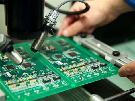
- Automated Optical Inspection (AOI): A camera-based system is used to visually inspect the PCB for defects such as missing or misaligned components, solder bridges, or incorrect component polarity.
- X-ray Inspection: For multi-layer PCBs or boards with hidden components, X-ray imaging is used to inspect the internal layers and solder joints for defects.
Boards that pass the electrical tests and inspections are then packaged and shipped to the customer for assembly. Boards that fail are analyzed to determine the root cause of the defect and either reworked or scrapped, depending on the nature and severity of the issue.
Frequently Asked Questions (FAQ)
1. What is the difference between a single-layer, double-layer, and multi-layer PCB?
- Single-layer PCB: A PCB with conductive copper traces on only one side of the substrate. Single-layer PCBs are the simplest and least expensive to manufacture but have limited routing options and are suitable only for simple circuits.
- Double-layer PCB: A PCB with conductive copper traces on both sides of the substrate. Double-layer PCBs offer more routing flexibility and can accommodate more complex circuits than single-layer boards.
- Multi-layer PCB: A PCB with three or more conductive copper layers, separated by insulating layers. Multi-layer PCBs are used for complex, high-density circuits and offer the most routing options and best signal integrity.
2. What is the purpose of vias in a PCB?
Vias are conductive holes drilled through the PCB that allow signals to pass from one layer to another. There are two main types of vias:
– Through-hole vias: Vias that go through the entire thickness of the PCB, allowing components to be mounted on both sides of the board.
– Blind and buried vias: Vias that connect only certain layers of the PCB, either starting or ending in an inner layer (blind) or connecting only inner layers (buried). Blind and buried vias are used to save space and improve signal integrity in high-density designs.
3. What is the difference between a plated through-hole (PTH) and a non-plated through-hole (NPTH)?
- Plated through-hole (PTH): A hole that is drilled and then plated with a conductive material (usually copper) to provide electrical continuity between layers. PTHs are used for mounting through-hole components and for creating vias.
- Non-plated through-hole (NPTH): A hole that is drilled but not plated with a conductive material. NPTHs are used for mounting purposes only, such as for mechanical support or for attaching heat sinks.
4. What is the purpose of solder mask on a PCB?
The solder mask is a protective coating applied to the copper traces on a PCB. Its Main purposes are:
– To insulate the copper traces from accidental contact and prevent short circuits
– To protect the copper from oxidation and corrosion
– To prevent solder bridges from forming between closely spaced pads during assembly
– To provide a finished, professional appearance to the PCB
5. What factors should be considered when choosing a surface finish for a PCB?
When selecting a surface finish for a PCB, several factors should be considered:
– Solderability: The surface finish should provide good wetting and spreading of solder to ensure reliable solder joints.
– Shelf life: Some surface finishes, like OSP, have a limited shelf life and may degrade over time, while others, like ENIG, offer a longer shelf life.
– Flatness: Surface finishes like ENIG provide a flat, planar surface that is ideal for fine-pitch components, while others, like HASL, can result in an uneven surface.
– Cost: The cost of the surface finish can vary widely, with options like HASL being less expensive than ENIG or IAg.
– Compatibility: The surface finish should be compatible with the types of components and assembly processes used, such as lead-free soldering or wire bonding.
By carefully considering these factors and the specific requirements of the PCB design, engineers can select the most appropriate surface finish for their application.

Leave a Reply