Table of Contents
- Design and Engineering
- Material Selection
- PCB Fabrication
- 3.1 Copper Clad Laminate Cutting
- 3.2 Drilling
- 3.3 Deburring and Cleaning
- 3.4 Electroless Copper Deposition
- 3.5 Dry Film Lamination
- 3.6 Exposure and Developing
- 3.7 Pattern Plating
- 3.8 Photoresist Stripping
- 3.9 Etching
- 3.10 Solder Mask Application
- 3.11 Silkscreen Printing
- 3.12 Surface Finish
- PCB Assembly
- 4.1 Solder Paste Application
- 4.2 Component Placement
- 4.3 Reflow Soldering
- 4.4 Inspection and Testing
- FAQ
1. Design and Engineering
The PCB manufacturing process begins with the design and engineering phase. This step involves creating a schematic diagram and converting it into a PCB layout using specialized software. The layout determines the placement of components, traces, and vias on the board.
2. Material Selection
Selecting the appropriate materials for the PCB is crucial for its performance and reliability. The most common base material for PCBs is FR-4, a glass-reinforced epoxy laminate. Other factors to consider include the copper thickness, dielectric constant, and thermal conductivity of the materials.
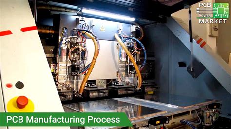
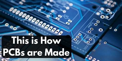
3. PCB Fabrication
3.1 Copper Clad Laminate Cutting
The fabrication process starts by cutting the copper clad laminate into the required board size. This is done using a specialized cutting machine that ensures precise dimensions.
3.2 Drilling
Holes are drilled into the board to accommodate through-hole components and vias. The drilling process is performed using high-speed CNC machines with drill bits of varying sizes.
3.3 Deburring and Cleaning
After drilling, the boards are deburred to remove any rough edges or burrs around the holes. The boards are then cleaned to remove any debris or contaminants.
3.4 Electroless Copper Deposition
To ensure proper electrical connectivity, a thin layer of copper is deposited onto the walls of the drilled holes using an electroless copper deposition process.
3.5 Dry Film Lamination
A photosensitive dry film is laminated onto both sides of the board. This film will be used to transfer the PCB layout pattern onto the copper layer.
3.6 Exposure and Developing
The PCB layout pattern is transferred onto the photosensitive film using UV light exposure. The exposed areas of the film are then removed using a developing solution, revealing the desired copper pattern.
3.7 Pattern Plating
Additional copper is plated onto the exposed copper areas to achieve the desired thickness. This process is known as pattern plating.
3.8 Photoresist Stripping
The remaining photoresist film is stripped away, leaving only the plated copper pattern on the board.
3.9 Etching
The unwanted copper areas are removed using a chemical etching process. This step defines the final copper traces on the board.
3.10 Solder Mask Application
A solder mask is applied to the board to protect the copper traces from oxidation and prevent solder bridging during the assembly process. The solder mask also provides insulation between the traces.
3.11 Silkscreen Printing
Text, logos, and component identifiers are printed onto the board using a silkscreen printing process. This step helps with component placement and identification during assembly and troubleshooting.
3.12 Surface Finish
A surface finish, such as HASL (Hot Air Solder Leveling), ENIG (Electroless Nickel Immersion Gold), or OSP (Organic Solderability Preservative), is applied to the exposed copper areas to prevent oxidation and enhance solderability.
4. PCB Assembly
4.1 Solder Paste Application
Solder paste is applied to the pads on the PCB using a stencil printing process. The solder paste contains tiny solder particles suspended in a flux medium.
4.2 Component Placement
Surface mount components are placed onto the solder paste using high-speed pick-and-place machines. These machines use computer vision and precision nozzles to accurately position the components.
4.3 Reflow Soldering
The board is then passed through a reflow oven, where the solder paste melts and forms a permanent connection between the components and the PCB pads.
4.4 Inspection and Testing
After assembly, the PCBs are inspected for any defects or misaligned components using automated optical inspection (AOI) systems. Functional testing is also performed to ensure that the boards operate as intended.
PCB Manufacturing Steps Overview
The following table summarizes the 17 common PCB manufacturing processing steps:
| Step | Process | Description |
|---|---|---|
| 1 | Design and Engineering | Creating schematic and PCB layout |
| 2 | Material Selection | Selecting appropriate PCB materials |
| 3.1 | Copper Clad Laminate Cutting | Cutting laminate into required board size |
| 3.2 | Drilling | Drilling holes for through-hole components and vias |
| 3.3 | Deburring and Cleaning | Removing rough edges and cleaning boards |
| 3.4 | Electroless Copper Deposition | Depositing thin copper layer onto hole walls |
| 3.5 | Dry Film Lamination | Laminating photosensitive film onto board |
| 3.6 | Exposure and Developing | Transferring PCB layout pattern onto film |
| 3.7 | Pattern Plating | Plating additional copper onto exposed areas |
| 3.8 | Photoresist Stripping | Removing remaining photoresist film |
| 3.9 | Etching | Removing unwanted copper areas |
| 3.10 | Solder Mask Application | Applying solder mask for protection and insulation |
| 3.11 | Silkscreen Printing | Printing text, logos, and identifiers |
| 3.12 | Surface Finish | Applying surface finish to prevent oxidation |
| 4.1 | Solder Paste Application | Applying solder paste to pads using stencil printing |
| 4.2 | Component Placement | Placing surface mount components onto solder paste |
| 4.3 | Reflow Soldering | Melting solder paste to form permanent connections |
| 4.4 | Inspection and Testing | Inspecting for defects and performing functional tests |
FAQ
1. What is the purpose of the solder mask on a PCB?
The solder mask serves two main purposes: protecting the copper traces from oxidation and providing insulation between the traces to prevent solder bridging during the assembly process.
2. What is the difference between through-hole and surface mount components?
Through-hole components have leads that are inserted into drilled holes on the PCB and soldered on the opposite side. Surface mount components are placed directly onto solder paste on the PCB pads and are soldered using a reflow oven.
3. Why is it important to clean the PCB after drilling?
Cleaning the PCB after drilling removes any debris or contaminants that could affect the subsequent manufacturing steps, such as electroless copper deposition and dry film lamination.
4. What is the purpose of the silkscreen printing step?
Silkscreen printing is used to add text, logos, and component identifiers to the PCB. This helps with component placement and identification during assembly and troubleshooting.
5. How are PCBs inspected for defects after assembly?
Automated optical inspection (AOI) systems are used to inspect PCBs for defects or misaligned components after assembly. These systems use high-resolution cameras and advanced image processing algorithms to detect any issues.
Understanding the PCB manufacturing process is essential for designers, engineers, and anyone involved in the electronics industry. By familiarizing yourself with these 17 common manufacturing processing steps, you can better understand the capabilities and limitations of PCB production, leading to more efficient designs and smoother collaboration with PCB manufacturers.

Leave a Reply