What are Molded Interconnect Devices?
Molded Interconnect Devices are three-dimensional (3D) injection-molded plastic parts with integrated conductive traces that replace the need for separate PCBs and mechanical components. The conductive traces are selectively applied to the surface of the molded plastic part, creating a compact and highly integrated device that combines both mechanical and electrical functions.
MIDs offer several key advantages over traditional PCBs and separate mechanical components:
-
3D design freedom: MIDs allow for complex, three-dimensional designs that are not possible with flat, two-dimensional PCBs. This enables more compact and efficient packaging of electronic components.
-
Reduced assembly steps: By integrating electrical and mechanical functions into a single component, MIDs reduce the number of assembly steps required, leading to faster production times and lower costs.
-
Improved reliability: The elimination of connectors and solder joints between separate components enhances the overall reliability of the device.
-
Miniaturization: MIDs enable the miniaturization of electronic devices by combining multiple functions into a single, compact component.
Manufacturing Processes for MIDs
There are several manufacturing processes used to create Molded Interconnect Devices, each with its own advantages and limitations. The most common methods include:
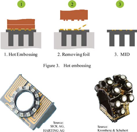
Two-Shot Molding
Two-shot molding, also known as 2K molding, involves injecting two different plastic materials into a single mold cavity. The first shot creates the base structure of the MID, while the second shot introduces a plastic material that can be selectively activated to create conductive traces. This process allows for the creation of complex, three-dimensional structures with integrated conductive paths.
Laser Direct Structuring (LDS)
Laser Direct Structuring is a popular method for creating MIDs. In this process, a thermoplastic material containing a special additive is injection-molded into the desired shape. A laser then selectively activates the additive, creating a micro-rough surface that promotes the adhesion of a conductive layer, typically applied through electroless plating. LDS offers high precision and allows for fine-pitch traces, making it suitable for high-density applications.
In-Mold Electronics (IME)
In-Mold Electronics is a relatively new process that combines printed electronics with injection molding. Conductive traces are printed onto a flat substrate, which is then thermoformed into a three-dimensional shape and placed into an injection mold. The plastic material is then injected around the substrate, creating a fully integrated MID. IME enables the integration of more complex electronic components, such as sensors and displays, directly into the molded part.
Applications of Molded Interconnect Devices
MIDs find applications in a wide range of industries due to their ability to combine mechanical and electrical functions into a single, compact component. Some of the most common applications include:
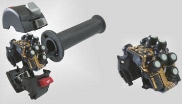
Automotive Electronics
MIDs are increasingly used in automotive electronics, particularly in sensor housings, lighting systems, and interior components. The 3D design freedom and reduced assembly steps offered by MIDs make them an attractive option for the automotive industry, where space constraints and reliability are critical factors.
| Application | Benefits |
|---|---|
| Sensor housings | Compact design, improved reliability |
| Lighting systems | 3D design freedom, reduced assembly steps |
| Interior components | Integration of electronic and mechanical functions |
Medical Devices
The medical industry has embraced MIDs for their ability to create compact, high-density devices with improved reliability. Applications include:
- Hearing aids
- Insulin pens
- Surgical instruments
MIDs enable the miniaturization of these devices while maintaining or improving their functionality and reliability.
Consumer Electronics
MIDs are used in a variety of consumer electronics applications, such as:
- Smartphones
- Wearables
- Smart home devices
The 3D design freedom and ability to integrate multiple functions into a single component make MIDs an attractive option for the consumer electronics industry, where device size and functionality are key factors.
Industrial Automation
In industrial automation, MIDs are used in sensors, actuators, and other control components. The improved reliability and reduced assembly steps offered by MIDs make them well-suited for the demanding conditions found in industrial environments.
| Component | MID Benefits |
|---|---|
| Sensors | Compact design, improved reliability |
| Actuators | Integration of electronic and mechanical functions |
| Control components | Reduced assembly steps, improved reliability |

Design Considerations for MIDs
When designing Molded Interconnect Devices, several key factors must be considered to ensure optimal performance and manufacturability:
Material Selection
The choice of plastic material is critical for the success of an MID. The material must be compatible with the selected manufacturing process and provide the necessary mechanical, thermal, and electrical properties. Common materials used for MIDs include:
- Polycarbonate (PC)
- Polyamide (PA)
- Liquid Crystal Polymer (LCP)
- Polyphthalamide (PPA)
Trace Design
The design of the conductive traces is another crucial aspect of MID development. Trace width, spacing, and thickness must be carefully considered to ensure proper electrical performance and manufacturability. The chosen manufacturing process will also influence trace design, as each method has its own limitations and capabilities.
Component Placement
The placement of electronic components on an MID must be carefully planned to ensure proper functionality and ease of assembly. Designers must consider factors such as component size, heat dissipation, and accessibility when determining the optimal placement of components on the molded part.
Simulation and Testing
Simulation tools, such as finite element analysis (FEA) and computational fluid dynamics (CFD), can be used to optimize the design of MIDs before prototyping and production. These tools help designers identify potential issues related to mechanical stress, thermal management, and electromagnetic compatibility. Thorough testing of prototypes is also essential to validate the design and ensure the desired performance and reliability.
FAQ
What are the advantages of MIDs over traditional PCBs?
MIDs offer several advantages over traditional PCBs, including 3D design freedom, reduced assembly steps, improved reliability, and the ability to integrate mechanical and electrical functions into a single component. These benefits lead to more compact, efficient, and cost-effective devices.
What are the most common manufacturing processes for MIDs?
The most common manufacturing processes for MIDs are two-shot molding, laser direct structuring (LDS), and in-mold electronics (IME). Each process has its own advantages and limitations, and the choice of method depends on factors such as design complexity, material requirements, and production volume.
What industries commonly use MIDs?
MIDs find applications in a wide range of industries, including automotive electronics, medical devices, consumer electronics, and industrial automation. The benefits of MIDs, such as compact design, improved reliability, and reduced assembly steps, make them an attractive option for these industries.
What materials are commonly used for MIDs?
Common materials used for MIDs include polycarbonate (PC), polyamide (PA), liquid crystal polymer (LCP), and polyphthalamide (PPA). The choice of material depends on the specific requirements of the application, such as mechanical strength, thermal stability, and electrical properties.
How can I ensure the success of my MID design?
To ensure the success of an MID design, several key factors must be considered, including material selection, trace design, component placement, and simulation and testing. By carefully addressing these aspects and working closely with experienced MID manufacturers, designers can create highly functional and reliable Molded Interconnect Devices.
Conclusion
Molded Interconnect Devices represent a significant advancement in the world of electronics packaging, offering a compact, efficient, and reliable solution for combining mechanical and electrical functions into a single component. By leveraging the benefits of 3D design freedom, reduced assembly steps, and improved reliability, MIDs enable the development of innovative products across various industries, from automotive electronics to medical devices and consumer electronics.
As technology continues to evolve and the demand for smaller, smarter, and more integrated devices grows, the adoption of MIDs is expected to increase. By understanding the manufacturing processes, design considerations, and applications of MIDs, engineers and product developers can harness the potential of this technology to create the next generation of electronic devices.
Leave a Reply